This thread has been locked.

If you have a related question, please click the "Ask a related question" button in the top right corner. The newly created question will be automatically linked to this question.

LM2904: LM2904

Part Number: LM2904
Other Parts Discussed in Thread: , , , , TLV9352-Q1, LM2903

We encounter a problem using LM2904BAQDGKRQ1(coding on circuit is 29Y0  2EMB) opamp.

This circuits are purchased from Mouser(595-LM2904BAQDGKRQ1).

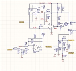
 In our schematic this is used to build a current source. 

 The problem is that the output voltage of the opamp (pin 1) is with 4.8V smaller than the power supply.

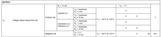
 In the datasheet this parameter is  around 1.4V.


  In the same datasheet there is LM2904AV that have the output voltage swing around 4V.

  • Please show the schematic.

    All LM2904 variants have pretty much the same output range.

      In the LM2904-Q1 we have different voltage swing output 

     -for LM2904-Q1, LM2904AV-Q1, LM2904V-Q1 we have 

    and for LM2904B-Q1 and LM2904BA-Q1 we have

    This means the output voltage swing are quite different.

  • The 1 nF capacitor at the output might make it oscillate. Please check with an oscilloscope. Otherwise, I see no reason why the output shouldn't be able to go higher.


    The datasheet values are different because the test load is different. The actual behaviour is similar (but the B variant is a little but stronger).

    The typical output behaviour is shown in figures 6-11/6-12 and 6-46/6-47. The graphs look different because of different scales, but the actual values of the curves are similar.

  • The output current in my schematic is almost 0 (gate of the PMOS transistor).

    This mean I should have at maximum 1.61V voltage swing according to your datasheet.

    But this is not happened...

    I have changed the opamp LM2904 with a different one (from ON semi) and the voltage output swing was ok (under 2V).

    Could you help me to understand this behavior?

    Thank you

  • Hi Marian,

    with a supply voltage of +23.8V and an input voltage of +23.7V you violate the common mode input voltage range of U500A. The maximum input voltage would be +21.8V here (+23.8V - 2V).

    Kai

  • Marian,

    When both inputs are above input common mode range, both input pins cutoff; so there is no input signal. 

    On the oldest design LM2904 that have the least balanced input stage, they will have output that goes high when both input are above the common mode range. LM2904B has well balanced input stage so output is unpredictable when both inputs violate the common mode range. 

  • Hello Ron,

    Does TI have an opamp that will behave similarly to LM2904DR2G in this application? AEC-Q100 is preferred

    Best regards, Antoine

  • Antoine,

    Temporary solution could be LM2904-Q1 (not B)  or the ON solution, but there is no data sheet claim for either that supports this (cutoff) operation. There may be a future day when this no longer works. Watch for PCN notifications. This is not the best idea.

    TLV9352-Q1 is a better solution. See figure 6-30 showing no phase reversal.  

  •  Hello Ron,

    Thank you for your feedback. 

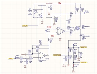
    I have made a change in the schematic and I wonder if this could work.

     Thank you

  • Hi Marian,

    you no longer have a connection to pin 3 of Q501?

    What are the red "GND" and "23V" labelings mean?

    Keep in mind that the maximum input voltage must remain 2V below the supply voltage of LM2903. See section 6.3 of datasheet. So, with a +24V supply voltage the maximum input voltage must not exceed +22V.

    Kai

  • Hello Kai,

    Thank you for your fast response.

    The pin 3 of Q501 is not connected in this version (it will be replace with a single transistor)

    GND is the voltage of the pin 3 of U500A (0V)

    23 V is the maximum voltage on pin 3 of U500A.

     The circuit is a current source. In normal working mode this work fine.

    The problem is when I have tried to disable the current source.  With the old circuit (in the beginning of this tread) the voltage of both opamp 

    inputs was exceeding the valid range. This is the reason that I change the disable circuit.

    You are right  the input voltage (in recommended  operating condition) should be maximum 22V.

    But in section 9.3.3 from datasheet we have:

      9.3.3 Input Common Mode Range
    The valid common mode range is from device ground to VS – 1.5 V (VS – 2 V across temperature). Inputs
    may exceed VS up to the maximum VS without device damage. At least one input must be in the valid input
    common-mode range for the output to be the correct phase. If both inputs exceed the valid range, then the
    output phase is undefined. If either input more than 0.3 V below V– then input current should be limited to 1 mA
    and the output phase is undefined ..

     In my understanding this circuit should work according to section 9.3.3.

     I have asked about these circuit because maybe I have not take in consideration all condition.

     Thank you

     Marian

  • Hi Marian,

    9.3.3 Input Common Mode Range
    The valid common mode range is from device ground to VS – 1.5 V (VS – 2 V across temperature). Inputs
    may exceed VS up to the maximum VS without device damage. At least one input must be in the valid input
    common-mode range for the output to be the correct phase.

    This only refers to the risk of "damage" or "phase reversal". But "no damage" and "no phase reversal" does not mean "linear operation". For linear operation both input voltages must be within the specified common mode input voltage range which is 0V...VS-2V.

    Kai 

  • Hello Kai,

    My intention was that the output of the U500A to go to high voltage (Vsupply-1.48V) in this operation mode with pin 2 to GND (disable current source).

    In normal operation mode (current source ) the voltage on opamp inputs are in the valid range.

    My question was if the pin 2 of the U500A go to  0V(GND) and pin 3 of the U500A go to 21V (in worst case 23V) the output can go to Vsupply -1.48V (like in the datasheet.).

    Thank you

    Marian

  • Marian,

    If pin 2 is 0V and pin3 > 0V then output should go high about VCC-1.5V

  •  Hello Ron

    Thank you for your support

    Marian

  • Hi Marian,

    as Ron answered, yes, the output should go high then, as explained in the datasheet. But keep in mind that the performance of LM2904 (refering to speed, etc.) will be degraded when leaving the common mode input voltage range.

    Kai