This thread has been locked.

If you have a related question, please click the "Ask a related question" button in the top right corner. The newly created question will be automatically linked to this question.

LM2903: The OPA output is abnormal, which makes the MCU unable to read and write.

Part Number: LM2903

Hi Team,

The current failure rate is 2500/2500, unable to write into the MCU, and the top image 28M still has 30K in stock.
There are currently 11 LOTs of 28M in stock, and each test of 10 units found the same loading condition, but the 27K/28K returned from the same batch did not have this problem.

This product is a digital meter case, which has been mass-produced for 4 years, and the design has not been changed during this period.

After checking, the OPA LM2903 output is abnormal, which makes the MCU unable to read and write. Test waveforms and the schematic are as the following.

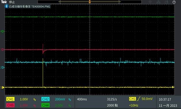
CH1:OPT_RXD, CH2:LM2903 Pin2, CH3:LM2903 Pin3, CH4:LM2903 Pin8_3.3V

  1. OK sample: OPT_RDX has an output signal
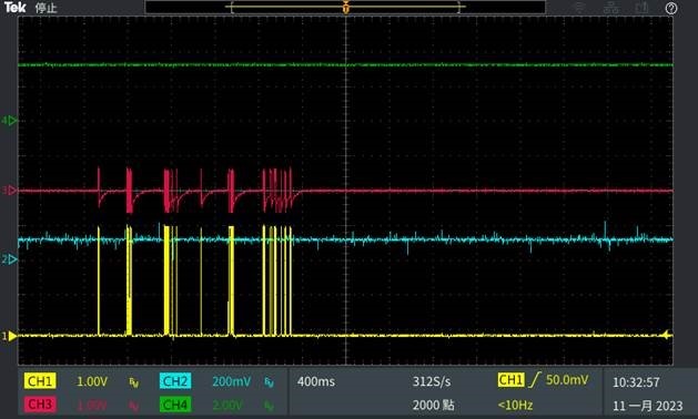

  2. NG sample: OPT_RDX no output signal
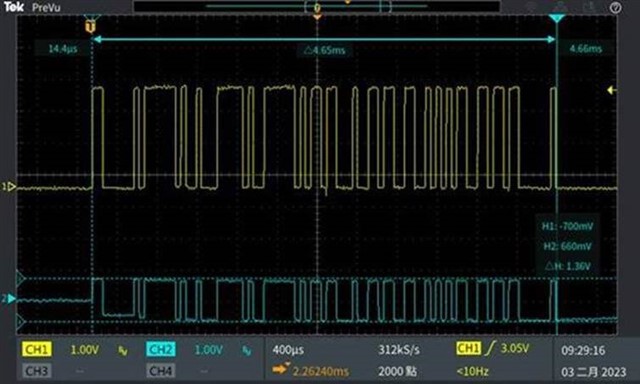
            

  • In both samples, the output goes high when the input goes high. I see nothing abnormal.

    The only visible difference is that in the second sample, there are fewer pulses. The LM2903 should not be able to affect its inputs; why are there fewer pulses? Is there no input signal at the phototransistor?

    (The reference voltage at pin 2 appears to be noisy; I would have added a small capacitor in parallel to R134.)

  • Hi Clemens,

    In both samples, the output goes high when the input goes high. I see nothing abnormal.

    ---May I know if the schmatic design is correct? 

    The only visible difference is that in the second sample, there are fewer pulses. The LM2903 should not be able to affect its inputs; why are there fewer pulses? Is there no input signal at the phototransistor?

    --- The customer checks the 5pcs NG(top image 28M) and good samples(top image 28K) for the A-B-A swap test in each same PCB, and we found the abnormal. 

    Regards 

    Rock

  • The schematic appears to be correct.

    Again, the only visible difference in these waveform is the input signal; both comparators behave the same.

    Please zoom in on one output pulse. What is the minimum pulse width required by the MCU?

  • Hi Rock,

    Thanks for reaching out. Yes the inputs seem to be very noisy and  is affecting the way the output is toggling. As Clemens mentioned, I would add the cap in parallel of R134 to stabilize the reference. The input waveforms look different between the two images so the output is toggling differently as well

  • Without C95, the signal would go above the valid common-mode range.

  • Thanks Clemens.  I completely agree, C95 blocks the DC portion of the input that would cause our device to see 3.3V directly instead of the pulses.  Here are a few comments.  It would make it easier to analyze the input condition for the comparator if both inputs were at the same volts/div on the scope and with their reference ground at the same position.  The smaller the differential becomes, you almost need a diff probe since the DC accuracy of oscilloscopes is not very good.  You may also want to increase the amount of hysteresis.  When the output changes states, 1M feedback resistor sees the 47.5k in parallel with 390.  So this is a very small amount of hysteresis. I am assuming the cap looks mostly like a short when the output switches.  Maybe try increasing the value of 390.  It is possible that some of your new LM2903 devices are part of our fab transfer and they are just more sensitive to small differences in the inputs.  Increasing the hysteresis may help.

    Chuck

  • Hi Team,

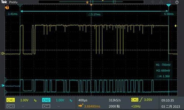
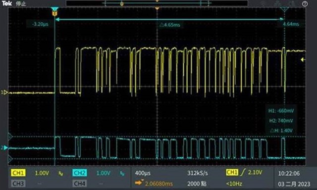
    Please Check the OK and FA PCBA functions of IC write.

    1) OK IC : CH1_Output to MCU, CH2_OPA input
    The output follows the input pulse, and the can be written successfully.


    2)NG IC : CH1_Output to MCU, CH2_OPA input
    Cannot output following the input pulse, and the written fail.

    Follow the suggestion, increasing the R130 to 2K and R126 to 180K. There have been some improvements but still writing fails.
    CH1_Output to MCU, CH2_OPA input

  • Rock

    Thanks for following up and sharing the new images.  These are much clearer.  I assume the light blue curve still shows the voltage at pin 3 of the comparator.

    Originally I believed D24 to be schottky diodes but after looking them up, it appears that they are just fast signal diodes with forward voltage drops in the 0.7V range.  This can cause a LM2903 to not function properly when the input is lower than -0.5V.  Any chance you could change D24 to a schottky?  This could be explaining why some lots are behaving differently than others.

    Chuck

  • Hi Chuck,

    After the customer checks, they change the diode with a forward voltage from 0.7V to 0.5V. Is this okay? Thanks.

  • Hi Rock,

    That is better. but you could also use a split resistor divider along with the diode to divide the signal further to be within the common mode range. Please see section 2.9.2.1 in Application Design Guidelines for LM339, LM393, TL331 Family Comparators (Rev. B)