Because of the Thanksgiving holiday in the U.S., TI E2E™ design support forum responses may be delayed from November 25 through December 2. Thank you for your patience.

This thread has been locked.

If you have a related question, please click the "Ask a related question" button in the top right corner. The newly created question will be automatically linked to this question.

PGA117: Data Sheet Questions

Part Number: PGA117

Hello Texas Instruments, 

1) If AVDD and DVDD are both 3.3V same exact voltage regulator part number but two different parts. Could this be a problem? Page 41 says make AVDD above DVDD so V out does not raise AVDD. I assume they will be within 10mV. 

2) What is the difference between binary and scope gain? I do not understand this and it is mentioned throughout the datasheet. 

3) What does the read command do? Check Table 4 for more info. 

4) If DVDD = AVDD = 3.3V is CH0 Reference a 3.0V reference ok? 

5) Can you confirm that VOUT is low impedance output capable of driving ADC? 

Thank You For Your Time. 

  • Hello, 

    I am also confused about the difference between what should be connected to VREF and CH0. 

    VREF => should this be connected to some lets say low reference voltage of 1.2V. Then a gain of 1 and 2 can be applied and the output offset drift and offset voltage can be calculated? Is this the VREF's main function? 

    CH0 => connected to 3.0V reference and depending on configuration (Table 10) the op amp outputs the fraction of the 3.0V reference. This is used to calibrate external ADC and any shifts in op amp? 

    Can you elaborate more on the difference between the two. 

    Thanks Again. 

  • Hi Brenden,

    Thank you for your interest in PGA117, I will try to address the questions from both of your comments in a single response. See below.

    1.) From page 41 of the datasheet: AVDD and DVDD can both be connected to the same supply; however, TI recommends using individual bypass capacitors directly at each respective supply pin to a single point ground. VOUT is diode clamped to AVDD (as shown in Figure 76); therefore, set DVDD less than or equal to AVDD + 0.3 V. DVDD and AVDD must be within the operating voltage range of 2.2 V to 5.5 V.

    2.) Binary gains are: 1, 2, 4, 8, 16, 32, 64, and 128; scope gains are: 1, 2, 5, 10, 20, 50, 100, and 200. These are the two gain ranges available depending on the part number PGA11x. PGA117 has the "scope" gain settings.

    3.) The read command allows you to read back the information that is written to the device registers, see section 8.6.3 of the datasheet.

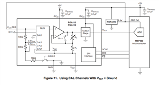
    4.) To use the CAL channels, VCAL/CH0 must be permanently connected to the system ADC reference, as shown in figure 71.

    5.) Yes, I can confirm the output is low-impedance and designed for driving ADCs, please refer to the datasheet for more information about ADC interfacing.

    6.) Vcal/CH0, the internal 10kΩ and 80kΩ resistors, and the internal CAL channels (see figure 71) are used to apply signals between 10% and 90% of the ADC reference voltage for calibration over the full-scale range of the ADC. Signals that saturate the output of the PGA117 at its minimum and maximum output swing are also applied for calibration.

    See Table 9 and Table 10, Table 9 illustrates how to use the CAL channels with VREF = ground. Table 10 describes how to use the CAL channels with VREF = AVDD/2.

    The purpose of Vref is to set the reference of your system, typically either GND or mid-supply.

    Regards,

    Zach