This thread has been locked.

If you have a related question, please click the "Ask a related question" button in the top right corner. The newly created question will be automatically linked to this question.

XTR111: Output current accuracy when differant room temp

Part Number: XTR111

Hi team,

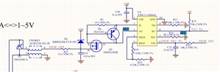
My customer uses XTR111 to design that to do tests when different room temp.

Remove R18 and connect to 5V. basically output current is 25mA.

So customer measures the current 24.857mA when TA=25C then TA up to 80C.

Current up to 25.563mA. the error around 2.8%. I ask customer to check the stability of 5V that only 0.1% drift.

So does any other possibility parameter affect the out current?


  • Hello Jimmy,

    A few questions:

    What is the VSP voltage ? Is the exposed thermal pad of the XTR111 connected to Ground? 

    What is the load resistance?  Is the load resistance referred to the same ground potential as the XTR111?

    Does the PCB board layout include a heatsink for the external P-FET transistor?

    How many PCB boards show this issue?  Can you share the PCB board layout Gerber plots?

    Were these PCB boards submitted to a typical solder reflow process and standard cleaning process or are they hand assembled? Flux often gets trapped underneath ICs where it can form undesired, parasitic capacitances and resistances.  These parasitic elements are often sensitive to temperature changes and often produce excessive leakage currents/drift on the circuitry, therefore, these errors could be related due to flux contamination. Consult the respective flux manufacturer or board assembly subcontractor, as proper flus removal may require use of a detergent based wash procedure.  For our lab PCB prototypes, we use a deionized water, an ultrasonic bath clean for 15 minutes, followed by a 75C oven bake-out for 30 minutes. The proper PCB cleaning process will depend upon the flux type you use. 

    What is the drift specification/part number of the RSET resistor?

    Thank you and Regards,

    Luis

  • Hi Luis,

    1. VSP is 15V

    2. Is the exposed thermal pad of the XTR111 connected to Ground?  ==>NO

    3. Does the PCB board layout include a heatsink for the external P-FET transistor? => YES

    4. How many PCB boards show this issue?=> total test 2 board

    5. Can you share the PCB board layout Gerber plots? => as below

    BTW, I do not understand why Flux will affect the output current. 

  • Hello Jimmy,

    The XTR111 thermal pad connection is missing on the design.   Please note, the XTR111 exposed thermal pad must be connected to GND to ensure correct/proper bias of the XTR111 internal circuitry.   Please modify the design to ensure the XTR111 thermal pad is connected to GND.  After modifying the PCB board design, connecting the thermal pad to ground, please re-attempt the tests using a new / fresh XTR111 device. The unit that was previously tested without grounding thermal pad could have been potentially stressed due to improper biasing, and may present degraded reliability.

    From p5 of the XTR111 datasheet:

    On the XTR111 circuit, the dominant portion of power dissipation for the current output is in the external FET.  It is important to consider the power dissipated by the external FET, which is a function of the power supply voltage, and current output range. It is a good idea to include an appropriate heatsink for the FET in the design. For example, the XTR111-2EVM incorporates the ZXMP6A13FTA P-Channel MOSFET on the SOT23-3 package. The XTR111-2EVM layout is shown on page 7 of the XTR111EVM User's Guide. The drain of the P-FET (pin2, pin4 heat sink) are connected to an isolated copper fill on Top and connected to another isolated copper fill on the bottom for heat dissipation.  

    Regarding the solder flux, if you are experimenting with prototypes and hand-soldering devices, please ensure to re-clean the PCB boards thoroughly removing any solder flux residue prior the drift test. Consult the respective flux manufacturer (or board assembly subcontractor), for proper flux removal procedure.  Solder flux often gets trapped underneath devices/ICs where it can form parasitic resistive (and capacitive) current paths.  These unintended parasitic resistance paths can cause leakage currents and are often sensitive to temperature, and produce unexpected errors/drift on the circuitry.  However, if your PCB board has already been gone through the solder flux clean process after installing/soldering devices, then this is not a concern, and please disregard this general comment.  In the circuit above, it appears the issue is related to the un-grounded exposed thermal pad.

    Thank you and Regards,

    Luis


  • Hi Luis,

    Got it. I will test again. thx for your support. 

  • HI Jimmy,

    Thank you, let us know if you have further questions.

    Best Regards

    Luis

  • Hi Luis,

    My customer tested again. but no any improve in current accuracy. so any new suggestions for us? thx 

  • Hello Jimmy,

    The XTR111 initial error at VIN=5V, IOUT = 24.467mA is relatively large and the drift errors are orders of magnitude larger than expected.  We have discussed the PFET transistor connections and heatsink.  Was the layout modified to correct the PFET transistor connections, add the PFET sink and the exposed thermal pad connection to ground on the XTR111 for these new tests?

    In order to help with the debug, please clarify the following:

    1) Kindly clarify: The DMP6250SE has two drain pins, pin 2 and heatsink pin as shown below.  Is pin (2) Drain connected in the layout above?  I can't immediately see a via connection on pin 2 on the layout.  Also, there is no heatsink copper fill shown on the layout above.

    2)  Please provide the new layout showing the XTR111 exposed thermal pad connected to GND.  If a second layer is available on the layout, kindly provide this Gerber plot as well.

    3)  What is the part number of the RSET resistor or what is the accuracy and drift spec in ppm/C of the RSET resistor?

    4) Can you please provide an explanation of the setup used to perform these tests.  What is the exact voltage measured with precision external meter across RSET when you get a reading of 25mA? Is this measurement performed with a precision voltage meter (6-digit)?  How are you measuring the output current, for example, are you using a resistor load referred to GND and measuring the voltage across the resistor?  What is the resistor tolerance and drift specification or what is the part number?  If measuring current directly with current meter, what meter is used to measure current?  Are these measurements all referred to the same local ground of the XTR111?

    5) If you use an oscilloscope to probe the XTR111, are there any oscillations at RSET (XTR111 Input) or at the drain of Q3 (XTR111 circuit output) that can be seen? If possible, please provide oscilloscope plots.

    Thank you and Regards,

    Luis 

  • Hi Luis,

    The XTR111 initial error at VIN=5V, IOUT = 24.467mA is relatively large and the drift errors are orders of magnitude larger than expected.  We have discussed the PFET transistor connections and heatsink.  Was the layout modified to correct the PFET transistor connections, add the PFET sink and the exposed thermal pad connection to ground on the XTR111 for these new tests?

    A: I measure current is 24.857mA, not 24.467mA. Also, customer is not re-layout at this moment. Just use a wire to connect GND. 

    1) Kindly clarify: The DMP6250SE has two drain pins, pin 2 and heatsink pin as shown below.  Is pin (2) Drain connected in the layout above?  I can't immediately see a via connection on pin 2 on the layout.  Also, there is no heatsink copper fill shown on the layout above.

     A: Pin2 of DMP6250SE just floating. 

    2)  Please provide the new layout showing the XTR111 exposed thermal pad connected to GND.  If a second layer is available on the layout, kindly provide this Gerber plot as well.

    A: customer is not re-layout at this moment. Just use a wire to connect GND.

    3)  What is the part number of the RSET resistor or what is the accuracy and drift spec in ppm/C of the RSET resistor?

    A: The REST P/N is ERA6AEB202V. 

    https://industrial.panasonic.com/ww/products/pt/high-precision-chip-resistors/models/ERA6AEB202V

    4) Can you please provide an explanation of the setup used to perform these tests.  What is the exact voltage measured with precision external meter across RSET when you get a reading of 25mA? Is this measurement performed with a precision voltage meter (6-digit)?  How are you measuring the output current, for example, are you using a resistor load referred to GND and measuring the voltage across the resistor?  What is the resistor tolerance and drift specification or what is the part number?  If measuring current directly with current meter, what meter is used to measure current?  Are these measurements all referred to the same local ground of the XTR111?

    A: I checked with the customer then measured voltage of RSET is 4.9678V when TA=25C.  Measured voltage of RSET is 4.9617V when TA=80C.

        You can see a very small drift on RSET setting. So should be other components or reasons to impact the current? 

      The customer uses CA310 of YOKOKAWA to measure current. Customer use  current meter then output short to GND then get output current.

    5) If you use an oscilloscope to probe the XTR111, are there any oscillations at RSET (XTR111 Input) or at the drain of Q3 (XTR111 circuit output) that can be seen? If possible, please provide oscilloscope plots.

    A: Waiting RD feedback. 

  • Thank you Jimmy,

    To answer your question, when the circuit is working as expected, in a proper board layout, the dominant sources of error is the accuracy and drift of the RSET resistor, and the small span error (0.015% typ, 0.1% max) , and span error drift 5ppm/C of the XTR111.

    In this case, after you have clarified/explained the input voltage conditions,  where RSET voltage is 4.9678V when TA=25C, this corresponds ideally to an output current of 24.839mA.  The customer measures 24.857mA when TA=25C which corresponds to an error of -0.07%.  The RSET resistor tolerance is 0.1%, so this falls under the expected accuracy at room.  However, the error of ~2.8% at 80C does not correlate to the expected performance of the XTR111 or RSET resistors.

    Board layout plays an important role in the performance: 

    The XTR111 thermal pad not only needs to be connected to ground, but soldering the exposed pad to the PCB is required, this significantly improves board-level reliability during temperature cycling.  In this case, when using the ground wire connection to the XTR111pad, please ensure the thermal pad still needs to be properly/evenly soldered to the PCB for good mechanical stability and reliability during temperature cycling. 

    Most of the power is  dissipated on the Q3 external transistor.  The power dissipated on the external transistor could approach 15V*25mA=0.375W continuous, therefore, in general we tend to recommend a conservative heatsink on Q3 to dissipate this power while providing this 25mA DC current. The heatsink plays an important role at the higher ambient temperatures. Please consult with the transistor manufacturer regarding the thermal resistance and minimum copper area heatsink requirements for this power dissipation condition, since the thermal package characteristics vary for different transistor manufacturers.  See XTR111 layout datasheet recommendations below:


    The bypass capacitor is missing on the XTR111 regulator.  The XTR111 datasheet requires a 470nF bypass capacitor for stability as mentioned in the datasheet.  This is missing on the schematic; and this could cause stability problems that could manifest intermittently on different conditions:

    A recommendation would be to improve the board layout: (1) adding the required 470nF bypass capacitor on the regulator, (2) add the XTR111 thermal pad ground connection, while providing both an electrical connection to ground and ensuring proper soldering of the XTR111 thermal pad to the PCB to ensure mechanical stability, and board reliability during temperature cycling and (3) Verify or consider improving the heatsink requirements on Q3 prior performing drift tests on the XTR111 module.

    Thank you and Regards,

    Luis