Part Number: PGA113
Other Parts Discussed in Thread: OPA325
Hi all.
I would like to use the PGA113 to set the first stage gain to the analog circuit on my sensor test board.
As you can see in the picture attached below, there are three different stages:
1) differential input stage
2) band-pass filter with two Sallen-Key stages
3) programmable amplier output stage
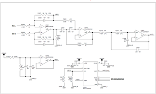
The supply VDDA_B is 3,3V. I got the VREF1 from VDDA_B with the resistive partitor R10-R11, so the VREF1 is equal to VDDA_B/2=1,65V.
In the PGA113 I only use one channel, so I put CH0 to GND with 1K resistor, as it was suggested from Luis in this discussion: PGA113: unused MUX pin termination.
I put VREF1 on pin 4 of PGA113 (pin VREF). Moreover the VREF1 voltage was applied to the differential input stage and to the first stage of band-pass filter.
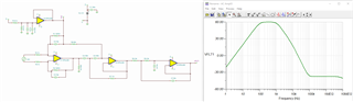
I can't simulate the entire schematic, because I don't find the PGA113 spice model.
Do you think the schematic is correct?
Thank you.
Gabriele.