This thread has been locked.

If you have a related question, please click the "Ask a related question" button in the top right corner. The newly created question will be automatically linked to this question.

INA280: bandwidth and output rise time

Part Number: INA280
Other Parts Discussed in Thread: TINA-TI,

Hi,

I want to estimate the rise time using the equation below.

tr= 0.35/bandwidth

Can I use the "Bandwidth" in datasheet for the denominator of the equation? I'm going to use A3 (gain of 50V/V). Then tr is going to be 0.38us. 

But what if Vsense is not 40mV? If Vsense changes, the bnadwidth also changes a lot? In system, Vsense keeps changing depending on the current across Rsns. 

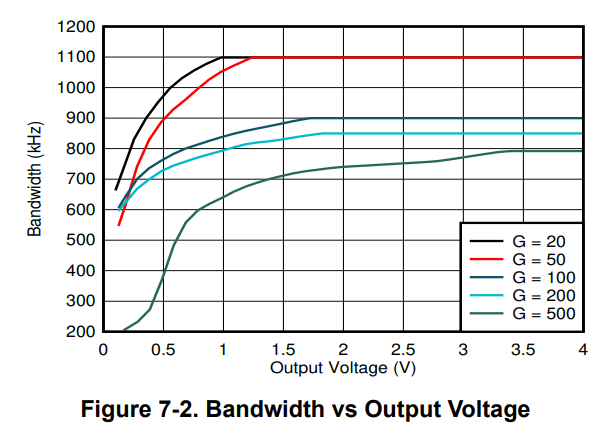
I also do not know how to select the "bandwidth" from Figure 7-2 for the denominator of the equation above. It varies depending on output voltage. But just like Vsense, output voltage keeps changing in system. Which "bandwidth" value should be selected for rise time estimation?
Thanks,

Ella

  • Hi Ella,

    why not looking at the slew rate which is specified to be 2V/µs? And figure 6-24 should help.

    Also have a look at the settling times which is 5µs for 1% settling and 9µs for 0.5% settling. The settling time gives you a good feel about how fast the output signal can follow the input signal.

    Or are you more interested in the small signal behaviour? Why not running a TINA-TI simulation?

    Kai

  • Hi Kai,

    Yes I'm asking this question to see the small signal behavior. I can run tina-ti sim but I also want to know the theory and simple calculation.

    Thanks!

    Ella

  • Hey Ella,

    The rise time equation (0.35/BW) I believe is based off an ideal, single-pole roll off frequency response. Even so, I would not use this to approximate INA280 rise or settling time.

    The frequency response BW specifications are tested with the Vout's DC components (or Vsense DC component) in the optimal range as shown in Figure 7-2. The BW for this device will change as the DC component of the input signal changes as shown in Figure 7-2.

    For these reasons, it can be difficult to approximate a rise time to a step response if Vsense is starting below the optimal DC operating point. The rise/settling time will also be worse if Vout is starting from 0V (saturation).

    The best way to use these BW curves is too establish if INA280 can drive an ADC, depending upon where Vout's DC component will at worst-case be at.

    For any step response where Vout is at least in linear region (>50mV), the Vout will respond with its current BW or go into slew mode depending on how large the step is. As Vout rises it's BW is increasing, so it will settle with the BW it has where Vsettle dictates settling BW according to Figure 7-2.

    Figures 6-24 and 6-25 can help provide some insight into these step responses, but overall a validation should always be considered and performed. You can use the simulation model, but unfortunately this BW vs. Vout_DC relationship is not modeled so the model will look better for these scenarios.

    Sincerely,

    Peter

  • Hi Ella,

    how small is your "small signal"?

    Kai