This thread has been locked.

If you have a related question, please click the "Ask a related question" button in the top right corner. The newly created question will be automatically linked to this question.

OPA2392: Input Bias Current question

Part Number: OPA2392
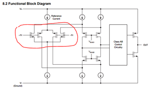
Other Parts Discussed in Thread: OPA2322, OPA2320, , OPA2328

Hello,

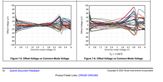
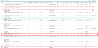
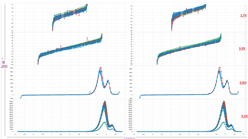
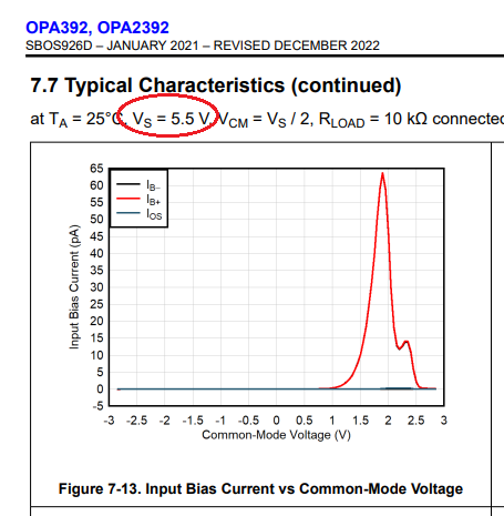
When looking at the Input Bias current vs Common mode voltage graphs, the third graph, which I assume is missing the Vs=5.5V marking has a very nasty increase between 1V and 2.5V.  Can you tell me if this chart is accurate?  It seems odd that additional supply voltage would create such a high input bias current (> 60 PicoAmps) when compared to the Vs=1.7 and Vs=3.3V graphs (30-40 FemtoAmps).

Thank You,

Ben

  • Hey Ben, 

    That is very likely correct as there is a crossover region where both polarities of input CMOS devices are on. This how you get RR input is pass control as some voltage between the inputs device, 

    This usually also shows up as an ugly step in input offset voltage, like this, '

  • I suppose I should have been more clear about what I'm really asking.  Being that the spike doesn't exist at Vs = 1.7 and 3.3V, It would be nice to know what the maximum Vs is before it appears.  I can reduce the Vs from 5V to something a bit less if it removes the Ib spike.

  • Hi Benjamin,

    a zero-crossover OPAmp like the OPA2320 or OPA2322 may be an alternative?

    Kai

  • Hi Benjamin, 

    Per Michael and Kai's comments, here are some precision op amps that may meet your application requirements, see TI E-store inventory. If you provide us with the op amp's BW and application, we may be able to find other alternative to replace OPA2392.  

    https://www.ti.com/amplifier-circuit/op-amps/precision/products.html#p2192=Zero%20Crossover

    If you have additional questions, please let us know. 

    Best,

    Raymond

  • Hello Raymond,

    OPA2328 is a good-looking part, I must say.

    That being said, OPA2392 checks a lot of boxes for this design - most notably it's size and very low Ib, especially over the full -40->125C temperature range.

    I can work around the Ib vs CMR issue if I can understand it.  My supplies can be shifted to place my signal under the crossover - I just need to be able to confidently predict where that is.

    Typically, I would expect that point be be somewhere around (V+)-1.8 or (V+)-2.0, which is exactly where it is on the graph of Vs-5.5V (2.75 - 2.0V = 0.75V)

    What I would like to understand is why the part is completely unaffected by crossover at lower Vs (3.3V and 1.7V).

    Is it possible that it's actually at [(V-) + 5.5V - 2.0V], which would explain why it's a non-issue at Vs=3.3?

    OPA2392 is a really nice part for my application - I just need to be able to understand where this crossover really lies mathematically.
    At Vs = +/-2.5V, for instance, does the crossover begin at [2.5 - 2.0V] = 0.5V, or does it begin at [-2.5V + 5.5V - 2.0V] = 1.0V, or is it somewhere else entirely?

    I did try to simulate the part, but it seems Ib is not correctly modeled in the SPICE file.  Ib scales linearly with input voltage from -55nA to 55nA

    Thank You,
    Ben

    P.S. Secondary question, on OPAx392 parts with an enable pin, must this pin be driven high to enable, or can it be left unconnected/floating?

  • Hi Ben,

    IB bump shown in Fig 7-13 is a direct result of impact ionization of P-channel input MOSFET transistors. Please note that graph shown in Fig 7-11, 7-12 and 7-13 apply only at 25C and IB roughly double every 10 deg C as shown in Fig 7-14. 

    As far as your question about the maximum supply voltage to avoid the large increase in IB vs Vcm, the safest would be to keep it at 3.3V where it is tested in production.  The increase is gradual and at 5V supply the peak is about 3.6pA - see below.  Judging by the IB vs Vcm graphs, keeping the supply below 4.25V should mostly eliminate the IB bump.

    Btw, in your original question regarding Fig 7-13, you refer to a "missing the Vs=5.5V marking" - as a general rule, default conditions stated at the top of the page apply to all graphs UNLESS otherwise noted on the graph itself. Thus, in case of Fig 7-13, with no condition on the graph, the default condition of 5.5V apply.

    As far as your question about OPAx392 enable pin, in order to assure proper operation it must be driven within 0.5V of positive rail.  Thus, if unused it's best to short it to Vcc - it should NOT be left unconnected/floating.

  • Thank you very much Raymond.  Very useful information.

    Have a great day,
    Ben

  • Joe, no problem  Good luck.