A related question is a question created from another question. When the related question is created, it will be automatically linked to the original question.
If you have a related question, please click the "Ask a related question" button in the top right corner. The newly created question will be automatically linked to this question.
Part Number: OPA858 Other Parts Discussed in Thread: THS4541
Hi Expert,
My customer is using OPA858 in optical module, OPA858 is not rail to rail device, we want to make output swing max, how to optimize the schematic? please give some advice.
With a high bandwidth requirement, the OPA858 can handle an input capacitance of around 4 to 5pF at 20kOhms. With the additional gain setting in the feedback, this value would decrease. I would recommend removing the gain switch and using the THS4541 to set the desired gain, or use a differential VGA/PGA (variable or programmable gain amplifier).
A high gain bandwidth amplifier such as the OPA858, will be susceptible to oscillations due to the additional parasitic of the switch in the feedback. Here are two e2e with more information and discussion:
Input current of 0.22uA to 88uA would work with the set voltage bias and looking at the input referred noise figure on the first page of the OPA858 datasheet. Then the rest of the gain for higher output voltage range requirements can be tuned with the THS4541 as mentioned above.
we also have some question based on the suggestion.
1. oscillations due to the additional parasitic of the switch in the feedback.
this E2E link has "You can try to add a small phase lead capacitance directly across the -input and output of OPAmp, not only across the gain setting resistors. If adding such a small cap will resuslt in a decrease of noise, you may have cured this instability."
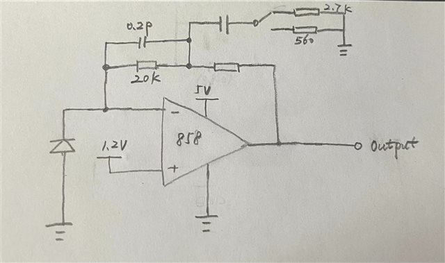
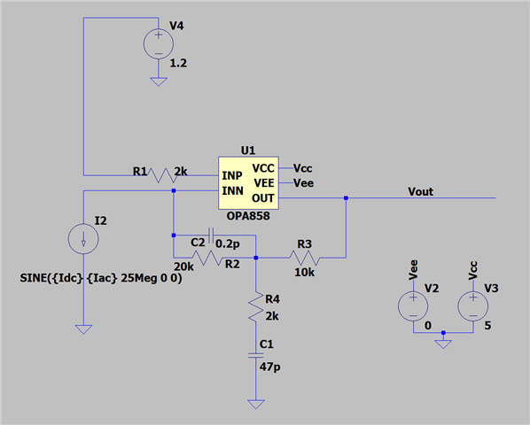
we assume the cap in the path of input and output so make a correction for schematic, could you help to review it? 1st is old one, 2nd is refreshed one.
2. it is better to add RISO between PD and IN- than PD directly connection IN-, my understanding is right?
we assume the cap in the path of input and output so make a correction for schematic, could you help to review it?
It's impossible to help without knowing the detector capacitance and the switch capacitances. So, please provide the detector capacitance and the switch capacitances or tell us what photodetector and what switch you are using.
the PD cap is 2pF. the Switch is NLAS7222BMUTBG、TS3USB30RSWR、SGM7222YWQ10/TR. please help to check the schematic.
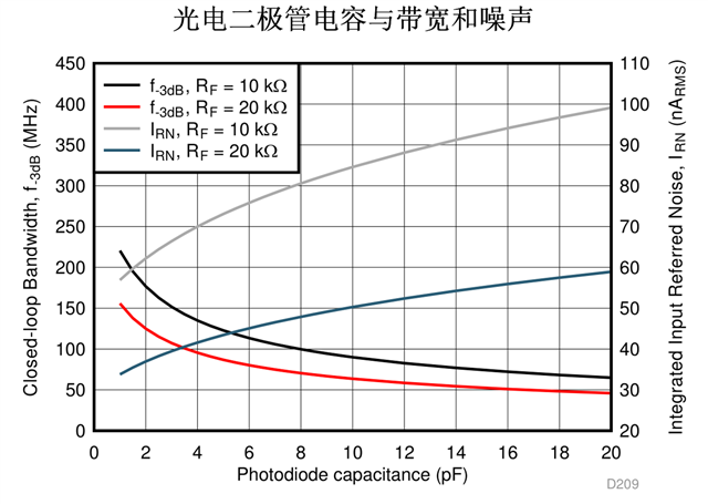
how to understand this "Input current of 0.22uA to 88uA would work with the set voltage bias and looking at the input referred noise figure on the first page of the OPA858 datasheet." could we take this picture as reference?
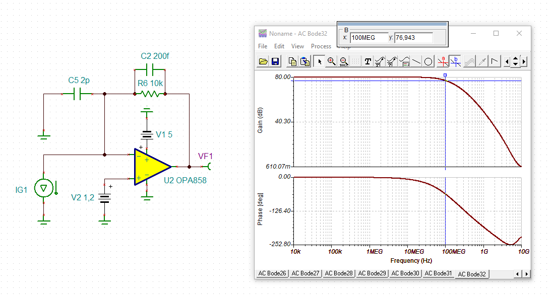
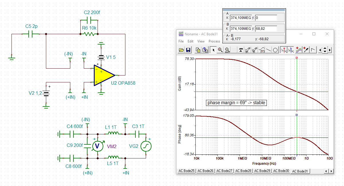
I'm sorry, I have run several simulations with your circuit but I was not able to achieve the wanted 100MHz bandwidth and to keep the OPAmp stable at the same time.
Also, even the least switch capacitance will considerably decrease the stability of your circuit. So, in any case the chosen USB switches will not work in combination with your circuit.