This thread has been locked.

If you have a related question, please click the "Ask a related question" button in the top right corner. The newly created question will be automatically linked to this question.

INA233: INA233

Part Number: INA233

Hello,

Designing with this part to measure the power used by a 12-24 watt motor,   the data sheet make a point of mentioning that inductive kickbacks need to be controlled with zener type devices good for positive going spikes, but I think we are also concerned with negative spikes, IN+ and IN-  have a limit of -0.3 volts, there does not seem to be a protective device for something that small.  We looked at the document referred to in the spec sheet listed below.

The Current Shunt Monitor with Transient Robustness Reference Design describes a high-side, current-shunt monitor used to measure the voltage developed across a current-sensing resistor and how to better protect the current-sense device from transient overvoltage conditions.  We do not think this will protect from negative spikes,  what do you suggest?   Are we being too cautious?  

I attached the reference document,  we not really clear on TP6 and TP7 do as it looks like that would ground the input, we assume it just a test point.  the interesting part is the 1 ohm with TVS and 9 ohm cap to ground.  I would like confirmation that this arrangement protect the chip and all we really need to do. 

thanks,

Gerard

TIDRDR7.PDF

  • Hello,

    Your concerns are correct. You must not violate the abs max but also you should not violate abs min. Having more than -0.3V on the pin will activate the ESD structure and can cause failure of the part. There are various ways to protect the device as you have mentioned. 

    I believe the TP6 and 7 are only test points and serve no protection purpose. 

    The best way to protect for negative voltage spike would be to use a Schottky diode from input pin to GND. Making sure the forward bias is less than .3V, they will activate before the device ESD diodes will creating the path for the current to travel rather than through the devices ESD structure.

    You may be overly concerned as one can consider current limiting resistors as enough protection for the device. Depending on the inductive kickback you would protect accordingly.

    Regards,

    Cas

  • Hello Castrense,

    Thanks for the reply,  we are thinking along the same lines of using Schottkey diode,   as you pointed out the Vf of the diode should be less than 0.3V,  that seems to be my problem,  i dont seem to find values less than 0.3V,  all the parts are silicon which pretty much makes them all about 0.3.   I have not found that Germanium based Schottkeys exist,  so if you are aware of a schottkey that is less than 0.3 volts and could point me to it I would be grateful.

    Regards,

    Gerard


  • Hello,

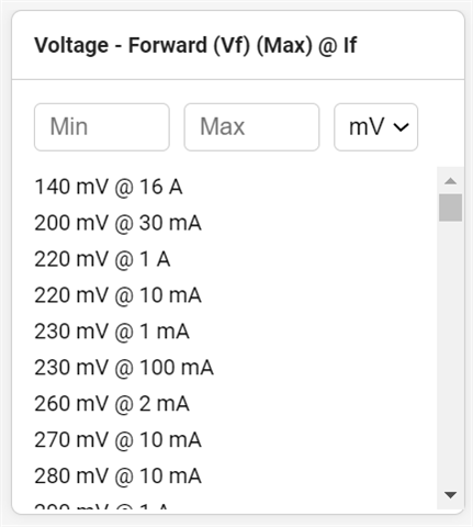
    I did a quick search on digikey and found this filter.

    I am not going to suggest one as I am unsure about other circuit parameters you are designing to but there are some Schottky diodes that can work.

    Regards,

    Cas

  • Thanks Cas,

    You answered the question,  I will assume that a higher current would be better, so something like the 203 mV at 100 mA would be best.  I am going to look for that device.

    Regards,

    Gerard

  • Hello,

    I believe that you will need a diode with a reverse diode voltage above your common mode voltage and probably above your high voltage protection. Yes I would agree that having higher current would be better.

    Regards,

    Cas

  • Hi Cas,

    There was only one option that had a low enough Vf and high enough Vrev, so thats what we went with.  

    Thanks for the help, i consider the matter closed.

    Gerard