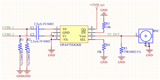
The OPA875 uses a single power supply input GND pin is also connected to GND.
1. What is the maximum resistance when the EN and SEL pins are pulled low and pulled high?
2. Is it necessary to add an isolation capacitor for CVBS input to V0 V1?
This thread has been locked.
If you have a related question, please click the "Ask a related question" button in the top right corner. The newly created question will be automatically linked to this question.
The OPA875 uses a single power supply input GND pin is also connected to GND.
1. What is the maximum resistance when the EN and SEL pins are pulled low and pulled high?
2. Is it necessary to add an isolation capacitor for CVBS input to V0 V1?

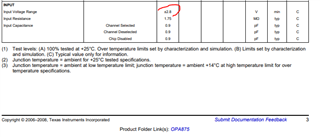
This will not work Terence, the inputs require 2.2V headroom to the supplies, you are at ground and don't have any bias path for the input currents, this is +/-5V supply specs. the inputs have a lot of headroom since this gain of 2 part will be overdriving the output if you actually input +/-2.8V.
Hi Michael :
If used divided by resistors to give a V0/V1 one DC level, can it conform to the requirement of +-2.8V?
Ps. CVBS 1/CVBS 2 is a 1V Vpp Video signal.
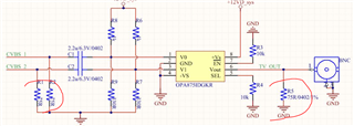
Is it this circuit as below which is correct?
yes, that should work, now, also, Increase R1 and R2 to 107ohms to maintain 75ohm match, also R5 is normally a series output 75ohm not shunt to ground,
Hi Michael:
The CVBS signal through the capacitor (CVBS1_1/CVBS2_2) is currently 2.8V at the DC level and the AC Vpp is 1V Vpp.
But the output(TV_out) still has no signal.
Is there any error with these circuits in my design?
Hello Terence,
When you mention there is no signal; is there any DC offset or clamping to either rail?
Also, what is the quiescent current or supply current when device is powered?
Thank you,
Sima
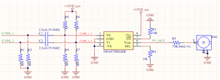
Both CVBS_1 /CVBS_2 and CVBS_1_2 /CVBS_2_2 have a DC level of 1V Vpp and an AC signal of 1V Vpp which is signal is the video signal of CVBS.
No matter if I pull EN and SEL high to 3.3V or GND, its Vout does not have any signal.
Unintentionally. I try the pin2 (GND) floating it.
The Vout began to have a signal output from CVBS_1/CVBS_2, but the signal at this time became has very noise on the CVBS signal.
thank you for your reply
Hello Terence,
Thanks for the additional tests and information! Based of the IC operation current, it could be the amplifier might have been damaged before schematic change to avoid violating the amplifier's input voltage range. Would you be able to replace the unit with a fresh unit? If board could not be modified to your updated schematic; as a quick test use a DC/AC signal as you mentioned above with the fresh unit.
Best Regards,
Sima
Hi Sima
This IC is broken maybe in operation over its spec.
And then I changed the new one and re-measure the operation current which the +Vs pin 12V output current has 5mA through in it.
Could you suggest the circuits, and how to use this IC in the operation mode in single power input or modify up to the circuits?
Thank you
Hello Terence,
I agree, but that is unusual that the fresh unit is not achieving the correct operation current. Your modified schematic is correct operation for single supply. Were you able to modify the board to include these changes (setting DC bias at input of amplifier)? If not, I would suggest removing the AC coupling capacitors and setting the correct DC bias via external equipment.
Thank you,
Sima
Hi sima,
Our initial design circuit is below the figure.
I measure each pin signal.
1.pin1 & pin3 is the 1V Vpp CVBS signal
2.pin5 SEL is low which is 0.4V
3.pin7 EN is low which is 0.4V
Would you suggest the circuit must modify where?
I tried to change the power supply to 12V.
Increase the DC level at the V0 &V1 to the OPA875 input and insert the capacitor for the CVBS signal to the island from the DSP CVBS signal.
But the output still doesn't have any waveform
Best Regards,
Hello Terence,
Thank you for the details. Is the additional capacitor for the CVBS signal a DC blocking/AC coupling capacitor?
Best Regards,
Sima
Hi Sima:
The additional capacitor is AC coupling capacitor for the CVBS.
And then I try to use another DC12V to supply OPA875 VS+(12V) VS-(GND).
But this power supply GND is not connected with CVBS GND,
The P6 Vout can output CVBS signal.
Is it the correct operation?
Best Regards,
Hello Terence,
CV_CVBS should be as shown in your last schematic with no AC coupling capacitor where the amplifier will see the DC bias for single supply configuration. For the new power supply, how is GND connected? It looks like you have a common ground connection between signals.
Thank you,
Sima
Hi Sima:
The OPA875 Vs+ Vs- power pin uses the power supply unit to supply, and the power supply unit negative is not connected to the system GND.
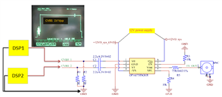
Hello Terence,
Thank you for the image! Does your PCB board have two different ground references/planes or VS- has its own connection on board indifferent to GND?
Thank you,
Sima
Yes.
Because in my experimentation. The Vs+ /Vs- of the OPA875 uses an external power supply unit to make the OPA875 work normally and Vout can output waveform. At this time, Vs- and the system GND are not connected together.
Conversely, if the power supply unit negative is connected to Vs- and the system GND. Vout cannot output any waveform.
Best Regards,
Hello Terence,
That is unusual; either this is from power supply or the amplifier does not work well when GND reference pin and VS- pins are shorted. It is probably the later; which would be a really good catch on the correct single supply configuration for this amplifier. I will need to confirm this with our design engineer, and get back to you. In the meantime, please measure the voltage seen at VS- pin of the amplifier just as a quick confirmation on supply's reference point.
Thank you,
Sima
Hi Sima:
Thank you for your reply
Finally, I tried to get the OPA875 working using dual power.
1. Use buck dc to dc to separate positive and negative 5V for OPA875.
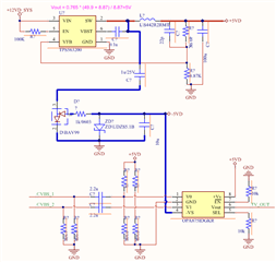
2. Use a Zener diode to make pin 2 GND of OPA875 form a floating. ground
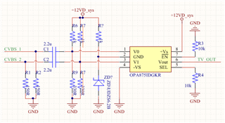
Best Regards,
Terence
Hello Terence,
I talked to our team, and it looks like the GND pin should have been named as a reference pin. Therefore, in single supply configurations, the reference should be mid-supply. For single supply configuration, it looks like from case 2 you found this out from setting GND pin to not ground. I am sorry for the confusion this has caused.
Thank you for the schematics. I am glad dual supply worked out!
Thank you,
Sima