This thread has been locked.

If you have a related question, please click the "Ask a related question" button in the top right corner. The newly created question will be automatically linked to this question.

TLV3604: Output of TLV3604 when input greater than 200 MHz.

Part Number: TLV3604
Other Parts Discussed in Thread: TLV3801, TLV3811, TLV3801EVM, TLV3601

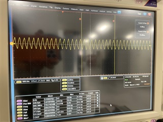
Output is square wave for input below 200 MHz and sawtooth when input greater than 200 MHz. Is this expected ?

Below are screenshots of TLV3604 outputs are different input frequencies - 

1. 100 MHz sinewave input

100 MHz TLV3604

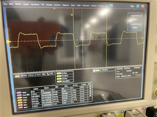
2. 200 MHz sinewave input

200 MHz TLV3604

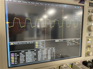
3. 300 MHz sinewave input

300 MHz TLV3604

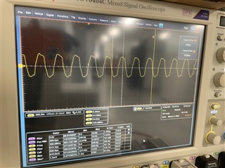
4. 500 MHz sinewave input

500 MHz TLV3604 output

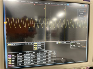
5. 900 MHz sinewave input

900 MHz TLV3604

In the final application, the input to TLV3604 will be pulses, as narrow as 1 ns, from photo-multiplier tube or ion detector and the output from the comparator will be sent to an FPGA for counting. My questions are - 

1. Is the behavior described and depicted in the screenshots above expected ?

2. If the behavior is expected, could you please recommend any other comparator part number that can go as fast as 1 ns.

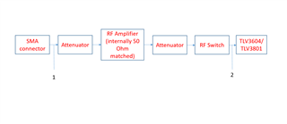
3. If the behavior is not expected, what could be some of the reasons for this ? I'm attaching the circuit schematic we're using and would appreciate feedback on it. 

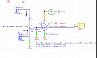
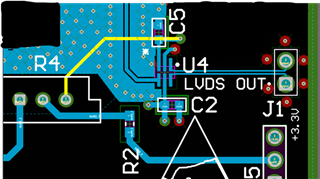
This circuit is completed in a 4-layer layout and fabricated. Please find layout screenshot attached here. In the screenshot –


  1. The Top layer (1) is blue, Ground (2) is green, Power (3) is red and Bottom (4) is yellow.  
  2. Input to TLV3604 (U4) pin 4 is single-ended coplanar 50 Ohm controlled impedance and has shielding vias on either sides. The reference ground plane for top layer is layer 2.
  3. Pin 1 of R4 pot is connected to ground  .
  4. J1 is a two pin male Molex header surrounded by ground vias.
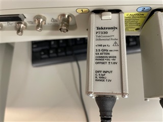
  5. All measurements are done by a scope with 100 Ohm differential probes.
  6. C2 is bypass capacitor for pin 5 placed as close to U4 as possible. It is 0.1 µF ±10% 50V Ceramic Capacitor X7R 0603 (1608 Metric).


Capacitor C5 is 0.1 µF ±10% 50V Ceramic Capacitor X7R 0603 (1608 Metric). I tried removing it from the board and the LVDS output looks the same as before where it was a square wave for frequencies below 200 MHz and sawtooth for frequencies above 200 MHz.

For prototype testing, the input is a sine wave but for the end application, the input will be short pulses with 1 ns pulse width.

Could you please provide feedback on how to achieve faster rise and fall times as close to the datasheet spec as possible. Please let me know if I can provide additional details. Thank you  


  • Raj

    thanks for posting to the forum. We are on holiday break today and will prepare a proper response tomorrow once we return. In the meantime, tlv3801 and tlv3811 are our fastest LVDS output comparators. Output response is very dependent on output load capacitance as well as the device’s speed capability. 
    Chuck

  • Adding differential probes info here.

    Differential Probes

  • Thanks for additional information. We’ve used a diff probe as well at different times. I want to say ours is 8GHz but I’d have to confirm. 

  • Hi ,

    Do you have an update on this ?

  • Raj

    Sorry for the delay.  In general, you are doing well with your setup and board layout.  At this frequency level, minimizing board parasitic capacitance on the input and output traces becomes more critical.  A technique we have learned over last iterations of board layout is to increase the spacing between the traces and ground pour on either side of the input and output traces to minimize parasitic capacitance.  See on our TLV3801EVM how this looks.  I don't see any shielding around your outputs and if the input is 50 ohm impedance, the output traces appear to not be impedance controlled which makes me concerned.  Your screen captures are not showing your input signal and I don't see any 50 ohm termination for your input.  I assume your high speed generator requires 50 ohm termination.  How is this being done.  When we characterize, we have a 50 ohm termination as close to the input pins as possible.  I also see how you are generating your reference with resistor divider.  Please note that the input bias current is in the uA range.  So kohm impedance can create mV's of offset shift. Maybe not critical for your circuit but just in case you input pulses decrease in amplitude, this could become important.  Please also tell me the reference voltage generated by the resistor network?  We test with low side threshold of approximately 300mV.  If you are at higher threshold, this could also limit the min pulse width capability.  I hate to turn you onto a different part but you are operating close to TLV3604 min pulse width operation.  The TLV3801 or TLV3811 would offer more headroom.  Lastly, we previously discussed your diff probe bandwidth.  At 3.5MHz, this starts to be a factor when detecting a 1ns pulse width.  Our diff probe is 8GHz.

    Chuck


  • Thank you for your response. 

    1. Shielding on outputs - Since the output signals are differential, they are routed as close to each other as possible and length matched. There's 100 Ohm termination close to the receiver, in this case, an FPGA. I see the output traces on TLV3801EVM split halfway and are no longer close to each other. Does this affect their ability to tightly couple with each other? We can add shielding on the outputs in the next iteration of this layout. Could you please share the layout and stackup files of this TLV3801EVM? I'm interested in looking at the trace width, dielectric type and height, ground polygon spacing and shielding via spacing. 

    2. Screen capture does not show input signal - The input sinewave is generated from a signal generator with 50 Ohm output and is connected to the DUT via an SMA connector. The trace from SMA connector to the input pin of TLV3604 is 50 Ohm single-ended coplanar waveguide with shielded vias on either side. The dielectric material used on this board is RO4350B.

    3. Reference voltage from resistor divider - There are two resistors in this divider circuit, 2 kOhm and 20 kOhm pot. We are testing with reference voltage in the range between 400 mV and 1 V, while the input signal is between 1 V and 2.6 V. 

    4. Regarding using TLV3801 instead of TLV3604 - I see the input voltage levels for TLV3801 for single supply are VEE + 1.5 V to VCC + 0.1 V. In our application, the reference voltage will be between 300 mV and 1 V and the input pulse level will be ~3 to 4 V. Given the high minimum input voltage requirement of TLV3801, do you have any suggestions on how to use it in our application?

    5. Is it possible to split the LVDS output such that one goes to an FPGA and the other goes to a testpoint for viewing on a scope? If yes, could you please recommend suitable parts and circuit. I did not find LVDS splitters in TI's product portfolio but I found one here MAX9175 670MHz LVDS-to-LVDS and Anything-to-LVDS 1:2 Splitters | Analog Devices and the only drawback is its max data rate is 800 Mbps.

  • Thanks Raj

    I will need to send friend request in order to send you the board file.  Board stack can be seen immediately in the user's guide.  In regards to the spreading of inputs and outputs, this was needed to accommodate the SMA connectors.  You mentioned that your source is 50ohm, so you will need a 50 ohm termination near the device input pins to terminate, otherwise you will have reflections.  I bring up the input because min pulse width is related to the width of the input compared to output.  You are correct that TLV3801 is not rail to rail, but it does allow for split supply operation.  For example, input stage can be powered from +/-2.5V and output can still be ground referenced to meet LVDS standard levels.

    Chuck

  • Thank you, Chuck. The input was missing a 50 Ohm termination resistor and after adding it, the output is much cleaner but the rise and fall times could still be better at higher frequencies. 

    I'm soon going to evaluate the TLV3801EVM as a potential replacement to TLV3604. I will be making VEE -2.5 V and VCC +5 V. This will allow the threshold voltage to be set between VEE + 1.5 to VCC + 0.1 = -0.5 V to 5.1 V and similarly the input pulse signal level can be between -0.5 V to 5.1 V. The output will be LVDS standard levels. Is this understanding correct?

    I would like to convert differential output of the comparator to single-ended LVTTL and connect to a 50 Ohm scope. Could you please recommend parts for achieving this. 

  • Raj,

    The supply voltage range for TLV3801 is defined by VCC - VEE = 2.7V to 5.25V. Therefore, the difference of +5V - -2.5V = 7.5V would violate this range. You need have your difference between the VCC and VEE levels be within the recommended supply voltage range. And the input voltage levels adjusted accordingly.

    You could convert the LVDS signal to a single ended output with another comparator such as TLV3601. 

  • Thank you, Chi. I'm evaluating TLV3801EVM and will update about the test results soon. 

    Thank you for recommending TLV3601 for LVDS to single-ended conversion. Its datasheet mentions maximum toggle frequency of 325 MHz. Will this be a bottleneck since TLV3801/TLV3604 LVDS outputs are much faster than 325 MHz.? 

  • Hi Raj,

    Sorry yes you're right. It will be limited by the toggle frequency and pulse width of the signal going into the TLV3601. Unfortunately we do not have a faster single ended output device that could handle that high of speed. 

  • Thank you, Chi. I found this LVDS receiver in TI's portfolio. SN65LVDS4 1.8-V High-Speed Differential Line Receiver datasheet (Rev. A) Can this be used instead?

  • Hi Raj,

    The front page states that its maximum signal rate is up to 500 Mbps, which correlates to ~ 250MHz toggle frequency signal.  Let me forward this thread to the appropriate team to help you with your part selection. 

  • Hello Raj,

    If I'm understanding the request correct, you are asking for a LVDS receiver to meet the TLV3801/TLV3604 toggle frequency? If so, our fastest LVDS receiver is the DS90LVRA2 with max signal rate of 600 Mbps (300 MHz). Otherwise, we don't have higher signal rate receivers.

    Regards,

    Josh

  • Hi Josh, thank you for the recommendation.

  • Hello Raj,

    No problem. Let us know if there's additional help that's needed.

    Regards,

    Josh

  • Hi Chuck, 

    This is the comparator input signal chain. Would you recommend having 50 Ohm termination resistor at location 1 or 2 or both? Will location 2 add an offset to the threshold voltage of the comparator?

  • Raj

    Thanks for the follow up.  Just want to make sure I am fully understanding the blocks because I am afraid that I am not following the diagram.  The signal comes into the board at an SMA, then it is attenuated, then amplified, then attenuated?  How is the attenuation accomplished?  Is this some sort of resistor divider network?  If so, I assume it is at least 10x or more higher than the 50ohm termination.  So position 1 is warranted.  But depending on what the termination looks like, I am not so sure position 2 will work.

    Chuck

  • The first is an RF attenuator (50 Ohm, 20dB). The second is also an RF attenuator (50 Ohm, 0 dB) for suppressing reflections. 

  • Raj

    The RF attenuators are already 50 ohm terminated, so an additional 50 ohm terminating resistor is not required in either location.

    Chuck