This thread has been locked.

If you have a related question, please click the "Ask a related question" button in the top right corner. The newly created question will be automatically linked to this question.

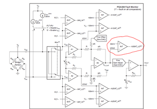
PGA308: A3SAT_LO fault resolution

Part Number: PGA308
Other Parts Discussed in Thread: , XTR116

Hello TI team,


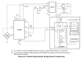
My application is very similar to Figure 6-3 of your publication “SBOU069B–June 2009–Revised January 2012” (i.e. TI PGA308 User Guide).

The only exception is the PGA308 is interfaced over 1 Wire via an Arduino Uno instead of the PGA308EVM.

The PGA308 is operating in Virtual Software Mode according to Figure 5-13 of the aforementioned publication.

Here is the output read from the microcontroller:

TIFL Register Value: 1100 1100 0000 0000

ZDAC Register Value: 0010 0001 0001 1001

GDAC Register Value: 1001 0101 1011 0101

CFG0 Register Value: 0011 1011 0000 0001

CFG1 Register Value: 0101 0000 0100 0000

CFG2 Register Value: 0000 1000 0000 0000

CHSR Register Value: 1011 0101 1110 1111

CHKS Register Value: 1011 0101 1110 1111

SFTC Register Value: 1000 0000 1000 0000

OENC Register Value: 0000 0000 0000 0000

ALRM Register Value: 0000 0000 0001 0000

OTPS Register Value: 0000 0000 0000 0000

With this implementation the A3SAT_LO bit (ALRM D4) is indicating a fault condition and the current returning to the XTR116 V+ pin is not changing in proportion to changing load of the bridge sensor.  The bridge sensor (a full bridge strain gauge load cell) is in working order as verified by an off-the-shelf load cell meter.

I read from page 40 of the aforementioned publication that: “The A3 amplifier in the Front-End PGA is also monitored for negative swing violations that can occur if the Zero DAC is incorrectly combined with the Front-End PGA gain select.”

I’m unable to figure out what if any error there is in the gain sizing & offset values.

I can send gain sizing & offset calculations in a direct email for your reference if required.

I have tried selecting FE_Gain on either side of the G_total but neither of these selections produce results that work.

Please advise on how the problem can be solved.


Thank you,

Robert Marvel
Electro-Mechanical Design Engineer

  • Hi Robert,

    The A3 internal amplifier block has an output swing limitation 50mV from the negative rail. If the voltage at the output of A3 is less than 50mV, the internal fault comparator will trigger the A3SAT_LO fault.

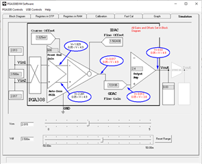
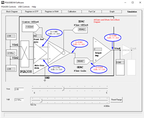
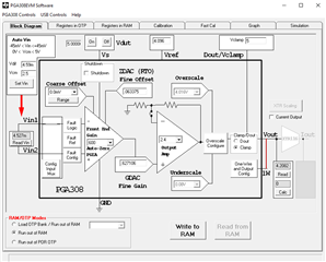
    The voltage at the output of A3 is determined by the input signal, the front-end gain, and the Zero DAC (fine offset adjust). The PGA308EVM software simulation tab is useful for simulating the internal nodal voltages depending on input and register settings. The example below with your gain settings shows that you will violate the A3 output swing limitation with an input of 3.5mV.

    From the diagram below, you may calculate the A3 output voltage by the following formula: VA3 = -(Diff_in - Coarse_Offset) * FE_Gain + ZDAC_RTO

    Note, if you switch the mux inputs the formula is VA3 = (Diff_in + Coarse_Offset) * FE_Gain + ZDAC_RTO

    Regards,

    Zach

  • Thank you for the help.  It turns out that VIN2 of the PGA308 was tied to ground inadvertently...  I have corrected that but now A1SAT_LO fault occurs.  Will you please help me out?  Here are my calculations & output:

    Inputs    
    Vs 5 V
    VREF 4.089 V
    Bridge_Offset 0.122279286 mV/V
    Bridge_Span 1 mV/V
    VEXC 4.089 V
    RBRG 1004 Ohm
    VOUT_MIN 0.5 V
    VOUT_MAX 4.21 V
    MUX 1 1, VINP=VIN1; 0, VINP=VIN2
    Step 0: Check load capablities of circuit PASS  
         
    Step 1. Calculate Zero and Full-Scale Bridge Sensor Input:    
    V_BR_MIN 0.0005 V
    V_BR_MAX 0.004589 V
         
    Step 2. Calculate Total Desired Gain:    
    G_total 907.3123013 V/V
         
    Step 3. Partition Total Desired Gain:    
    Initial Gain_DAC 0.666666667 (midscale gives most flexibility)
    FE_GAIN 800  
    OUT_GAIN 2 1066.666667
         
    Step 4. Calculate Gain DAC Values:    
    Gain_DAC 0.567070188  
         
    Step 5. Calculate Coarse Offset:    
    Table 7-37 A0 0.032  
    Table 7-37 A1 4  
    Coarse Offset Resolution 0.00102225 V
    Coarse Offset Range (+/-) 0.102225 V
    Coarse_Offset -0.00102225 V
    V_BR_MIN+Coarse_Offset -0.00052225 V
    residual error <= Coarse Offset Range TRUE  
         
    Step 6. Calculate Zero DAC:    
    Zero_DACx 0.858662534 V
         
    Step 7. Computed Values Check:    
    VOUT_MIN_compute 0.5 V
    VOUT_MAX_compute 4.21 V
         
    Step 8. Measured Values:    
    Program the PGA308 with computed values and take real-world measurements for VOUT_MIN at VBR_MIN and VOUT_MAX at VBR_MAX    
    VOUT_MIN_measure 0.5 V
    VOUT_MAX_measure 4.214 V
         
    Step 9. Adjusted VBR inputs:    
    Refer all errors between the ideal VOUT and measured VOUT to the input for a final calibration of Gain DAC and Zero DAC    
    VBR_MIN_measure 0.0005 V
    VBR_MAX_measure 0.004593409 V
         
    Step 10. Calibrated Gain DAC Values:    
    G_total_measure 906.3351206  
    Gain_DAC_calibrate 0.56645945  
         
    Step 11. Calibrated Zero DAC Values:    
    Zero_DACx_calibrate 0.859137857 V
         
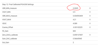
    Step 12. Final Calibrated PGA308 Settings:    
    VBR_MIN_measure 0.0005 V
    VOUT_MIN 0.5 V
    VBR_MAX_measure 0.004593409 V
    VOUT_MAX 4.21 V
    VEXC 4.089 V
    Coarse_Offset -0.00102225 V
    FE_Gain 800  
    Zero_DACx_calibrate 0.859137857 V
    Gain_DAC_calibrate 0.56645945  
    Out_Gain 2  
         
    Step 13. For final calibrated settings, check the internal PGA308 nodes for design margin:    
    (a) Front-End PGA Inputs (refer to Figure 3-5):    
    VINP_MIN 2.044238875 V
    VINP_MAX 2.046285579 V
    VINN_MIN 2.044761125 V
    VINN_MAX 2.042714421 V
    0.2 ≤ Linear Input Voltage Range ≤ VS – 1.4V TRUE  
    (b) A1, A2 Outputs (refer to Figure 3-2):    
    G = 1 + 2 RF/RG 200 (A3 has gain of 4)
    VCM_MAX 2.0445 V
    VDIFF_MAX 0.003571159 V
    VCM_MIN 2.0445 V
    VDIFF_MIN -0.00052225 V
    VOA1_MIN 1.992275 V
    VOA2_MIN 2.096725 V
    VOA1_MAX 2.401615863 V
    VOA2_MAX 1.687384137  
    0.1V ≤ VOA1, VOA2 ≤ VS – 0.12V TRUE  
    (c) A3 Outputs (refer to Figure 3-2):    
    VOPA_MIN 0.441337857 V
    VOPA_MAX 3.716064757 V
    0.05V ≤ VOPGA ≤ VS – 0.1V TRUE  
    (d) Output Amplifier Input (refer to Figure 3-3):    
    VOP_MIN 0.25 V
    VOP_MAX 2.105 V
    0V ≤ VOP ≤ VS – 1.5V TRUE  
    (e) Output Amplifier VOUT (refer to Figure 3-3):    
    0.1V ≤ VOUT ≤ VS – 0.1V (for 4mA source/sink) TRUE


    TIFL Register Value: 1100 1100 0000 0000
    
    ZDAC Register Value: 0100 1010 0011 0111
    
    GDAC Register Value: 0101 1001 1000 0110
    
    CFG0 Register Value: 0001 1100 1000 0001
    
    CFG1 Register Value: 0101 0010 0100 0000
    
    CFG2 Register Value: 0000 1000 0000 0000
    
    CHSR Register Value: 1110 0101 1000 0000
    
    CHKS Register Value: 1110 0101 1000 0000
    
    SFTC Register Value: 0000 0001 0000 0000
    
    OENC Register Value: 0000 0000 0000 0000
    
    ALRM Register Value: 0000 0000 1000 0000
    
    OTPS Register Value: 0000 0000 0000 0000


    Thank you,

    Robert
  • Hi Robert,

    Thank you for the detailed information. I believe your calculations have a sign error with respect to the differential input. From your table, the output of the bridge sensor is specified from 5μV to 4.59mV. Elsewhere in the table you specify the minimum differential input as -5μV.

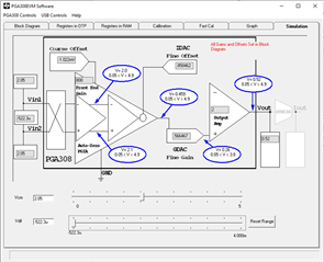
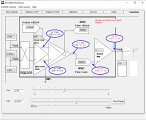
    It seems that your device is calibrated to output 0.5V for a differential input of -5μV, and as the differential input voltage increases (becomes more positive) the output voltage is driven into the negative rail. See simulation results below.

    Regards,

    Zach

  • Robert,

    Quick correction, I accidentally wrote 5μV and -5μV where I meant 500μV and -500μV.

    My apologies for the confusion.

    Regards,

    Zach

  • Hi Zach,

    I considered the first point you made about the bridge sensor output being different from VDIFF_MIN.  That is correct, the two are different because the VDIFF_MIN has the coarse offset applied to it whereas the bridge sensor output, of course, does not.  This is why you see the difference in the two values.  For curiosity, I changed the coarse offset to zero so that Bridge sensor output = VDIFF_MIN however the problem (i.e. ALRM bit 7 indicates A1SAT_LO fault) still persists.

    As for the second point you raised, I don't know why your simulation shows a negative correlation between differential input voltage & VOUT.  Do you suspect the findings from your simulation are indicative of why there is A1SAT_LO fault for my application?  If so, will you please elaborate more?

    Thank you,

    Robert

  • Hi Robert,

    I see I was misreading Vdiff as Vbr. Vdiff = (VinP-VinN). Therefore your values for Vdiff are correct as Vdiff_min = -522μV and Vdiff_max = 3.57mV. Of course, Vdiff is calculated after your 1.025mV offset correction is applied.

    If your measured bridge offset is 500μV, why are you using a coarse offset of 1.025mV? Your resulting offset is -522μV, therefore you are actually adding a higher magnitude error to your input. If coarse offset correction is set to 0, your bridge sensor output is 500μV to 4.59mV.

    As your bridge sensor output is a positive voltage, why are you setting the mux to 1? The purpose of the mux is to accommodate sensors with negative voltage outputs. The negative correlation between the output and the input is due to the mux polarity reversal.

    I recommend setting your coarse offset to zero volts and setting the mux logic to 0.

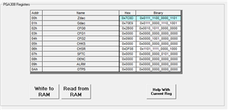
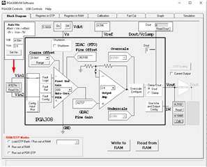
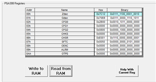
    Using the sensor emulator on the PGA308EVM, I was able to calibrate an output of 0.5V to 4.21V with a sensor input of 0.5mV to 4.59mV. I included my register values and gain settings below for reference, of course your final calibrated settings will be slightly different.

    Regards,

    Zach

  • Hi Zach,

    I take your point about using zero offset, notice in my last reply that I had already implemented that change :).

    As for the polarity versus mux, for my application I have positive polarity for Vin1 (i.e. positive voltage from bridge output going to Vin1).

    I believe your simulation uses negative polarity at Vin1 (which to your point the mux bit would then be 0)

    Nonetheless, I tried using your suggestion for mux = 0 for my application & it did not turn out well:

    TIFL Register Value: 1100 1100 0000 0000
    ZDAC Register Value: 0111 1100 0000 1101
    GDAC Register Value: 0111 0000 1110 1001
    CFG0 Register Value: 0010 1011 0000 0000
    CFG1 Register Value: 0000 0000 0000 0000
    CFG2 Register Value: 0000 1001 0000 0000
    CHSR Register Value: 1101 1111 0000 1000
    CHKS Register Value: 1100 1111 0000 1000
    SFTC Register Value: 1111 1111 1111 1111
    OENC Register Value: 1111 1111 1111 1111
    ALRM Register Value: 1111 1111 1111 1111
    OTPS Register Value: 1111 1111 1111 1111

    At this point I restored polarity back to Vin1 = Vinp (MUX = 1).

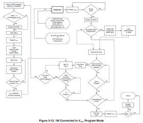
    I noticed that your simulation CHKS register has the value 0x00 which if I understand correctly from the flow chart (Figure 5-13 from the aforementioned TI publication) would give "No" for the decision point "CHSR Matches CHKS?" resulting in the process going into Standalone Mode.  After a "yes" to valid power in Standalone Mode one wire is enabled & then "BANK SELx programmed" decision is made, which in our case should be "No".  At this point Vout is disabled.  Here is where it gets tricky, it seems with CFG2 Register digit 8 flipped to high (DOUT SEL = 1 for Digital output function) & CFG2 digit 7 flipped low (DOUT = 0 or low logic output) the ALRM register returns all zeros in both my application & your simulation.

    However, if in my application I follow Figure 5-13 & write a valid CHKS (CHKS = CHSR) and us Vclamp function instead of Dout (i.e. DOUT SEL = 0) then the problem of A1SAT_LO reappears as before even when using the same ZDAC, GDAC, CFG0 & CFG1 register values as you used in the simulation.

    It seems that the problem still persists but I'm not sure where to go from here.

    I would appreciate your help on how to solve this.

    Respectfully,

    Robert

  • Hi Robert,

    My configuration registers will be different from yours as I am using the PGA308EVM to perform the calibration in software lock mode. Notice that 101 is written to the SWL bits of the SFTC register. In software lock mode the checksum is ignored, see figure 5-14.

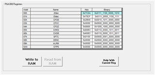
    I went back and calibrated the device using the VCLAMP function instead of DOUT. Please refer to ZDAC, GDAC, CFG0, CFG1, CFG2 registers.

    What potential is your Vclamp pin connected to? Can you provide a schematic of your board? Are you using 3-wire or 4-wire configuration?

    I believe in your recent test something was not configured properly as the SFTC, OENC, ALRM, and OTPS registers should not be set to all 1's. Simply toggling the mux and/or Dout should not have this effect on these registers 

    Do you have any insight on why these registers are configured this way? I am sure if we keep trying we can find the solution.

    Thanks,

    Zach

  • Hi Zach,

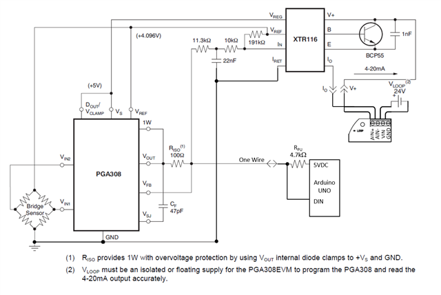
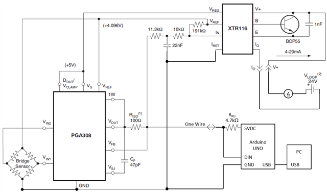
    Here is the circuit, as you can see it is 3 wire configuration with Vclamp at 5V, the loop is powered by a floating supply with current sensing capability:

    I don't know why SFTC, OENC, ALRM, and OTPS registers are returning values in the manner that they are.  Strictly speaking this is what I observed:

    Case 1:  When MUX bit is set to logic low then after the CHKS = CHSR check happens, everything is pulling back up to logic high regardless of what was requested during register writes.  In any case, I did not set the registers to all logic high, I requested they be set with the values you used in the simulation (including the SFTC SWL 101).

    Case 2: When MUX bit is set to logic high (as is the correct polarity for my application) and CHKS=CHSR, the register reads return the values as expected (i.e. to the requested set values).  This is where the ALRM register for A1SAT_LO occurs.

    Case 3: When MUX bit is set to logic high and CHKS=CHSR and CFG2 DOUT SEL = 1 and CFG2 DOUT = 0, I observed SFTC, OENC, ALRM, and OTPS registers all go to 0x00 including the ALRM and SFTC SWL bits.

    I can't explain why the PGA308 is behaving this way but I hope the observations provided will help us solve the issue.

    Regards,

    Robert

  • Hi Robert,

    I think I see the confusion, I was operating in the 4-wire configuration using the Software Lock Mode (SWL = 101), Figure 5-14. In four-wire mode, Vout can be enabled while communicating on the one-wire bus. In your 3-wire configuration Vout must be disabled during one-wire communication. When you set up your device using my register configurations you enabled Vout (CFG2 [D13] = 0), which is why your register reads showed all logic high.

    I tested my calibration again using the 3-wire configuration with Vclamp and the mux set to 0 for my polarity. You may refer to my gain and offset settings below, note that these settings are very similar to the previous 4-wire calibration settings. Also keep in mind that these register values are post-calibration, where the CHSR matches CHKS, Vout is enabled, and the one-wire is disabled. You may need to configure some registers differently during your test.

    Can you attempt this again in virtual software lock mode (SWL=000)? I recommend switching the mux polarity and monitoring the output voltage (with Vout enabled) while applying a signal near the middle of your input range such as 2mV.

    Thank you for providing the block diagram of your circuit, can you provide a schematic as well? I do not see ground or supply connections for your Arduino. The arduino ground must be connected to the Iret floating ground node as shown in figure 6-3, to ensure that the one-wire digital communication shares a common reference.

    Thanks,

    Zach

  • Hey Zach,

    Here is the output when I tried your suggestion:

    TIFL Register Value: 1100 1100 0000 0000
    
    ZDAC Register Value: 0111 1100 0000 1010
    
    GDAC Register Value: 0111 0000 1100 1111
    
    CFG0 Register Value: 0011 1011 0000 0000
    
    CFG1 Register Value: 0000 0000 0000 0000
    
    CFG2 Register Value: 1000 1000 0000 0000
    
    CHSR Register Value: 0101 0000 0010 0101
    
    CHKS Register Value: 0101 0000 0010 0101
    
    SFTC Register Value: 0000 0000 0000 0000
    
    OENC Register Value: 0000 0000 0000 0000
    
    ALRM Register Value: 0000 0000 0000 0000
    
    OTPS Register Value: 0000 0000 0000 0000


    Still there is no detected current returned to V+ of XTR116.

    Also, I do have IRET tied to Arduino Uno GND pin.


    Thanks,
    Robert
  • Hi Robert,

    It appears that your low saturation errors have been resolved and your alarm register is returning all 0. Are you able to measure the expected output voltage at the PGA308 VFB pin?

    If you require support with your current transmitter, I will need a detailed schematic showing all of the power supply and ground connections. If you are using a PCB design software, a screen capture of your full schematic diagram is sufficient. If you are not comfortable posting your full schematic on the public forum, you may send it to me directly for review. You can send me a direct message by pressing the "connect" button when viewing my profile on E2E.

    Thanks,

    Zach

  • Zach,

    Yes, I would appreciate support for the XTR116.

    The measured output at the PGA308 VFB pin to ground is 134.9 mV.

    From VOUT pin of PGA308 to ground is 15.3 mV.

    VIN2 - VIN1 = 0.6 mV.

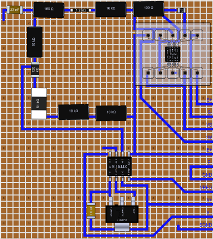
    The best I can do in providing a diagram showing power & ground connections is this:

    Believe or not I used SolidWorks to layout the board:

    For the PCBA outputs, VREG & VS are jumpered, GND, SGND (IRET) & the Arduino UNO GND pin are all jumpered.

    This was built on a SMT breadboard with plated through holes (depicted as circles) which make continuity with the back plane that I'm using as SGND (IRET).

    Thanks,

    Robert

  • Hi Robert,

    Thank you for providing this additional information. I have many concerns about this implementation.

    First, you will not be able to resolve your target sensor output of 0.5mA-4.59mA using a breadboard implementation of the PGA308. Breadboards are great tools for "quick and dirty" circuits, but they are useless for precision circuits such as the one you are attempting to design. Breadboards track resistances can be very high and also have parasitic capacitance and inductance. These breadboard parasitics generate compounding errors in your circuit that will make the desired level of precision impossible.

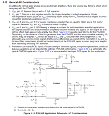
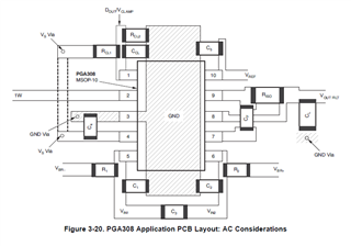
    Please refer to section 3.10 of the PGA308 user's guide, "General AC Considerations", for the recommended analog layout and design practices. Figure 3-20 of the PGA308 user's guide shows an example PCB layout. If possible, I recommend using the PGA308EVM along with your sensor and controller to prove your design concept, then design a PCB that will meet your performance requirements.

    I have additional concerns about your XTR implementation and ground connections, but we will need to resolve the PGA308 circuit first and ensure we are getting the correct output voltage before we can attempt to produce a useful 4-20mA signal. I recommend disconnecting the XTR from your PGA308 circuit for now, and use bench supplies for Vs, Vref, and your sensor excitation. Once the PGA308 circuit is functioning, calibrated, and producing the desired output voltage, we can revisit the XTR portion of the circuit.

    Note that the PGA308EVM has an XTR116 4-20mA loop onboard that may be a useful reference while you are designing your similar circuit. The PGA308EVM is in stock and available at the following link: https://www.ti.com/tool/PGA308EVM#order-start-development

    Thanks,

    Zach

  • Zach,

    I'm not sure that you understand what I meant by SMT breadboard.  An SMT breadboard is a PCB board that has isolated "copper pads" arranged in a grid pattern, spaced by 0.05" in my case, that serve as a generic land pattern for SMT components to be soldered to. The SMT breadboard I used has GND vias as shown in the User Guide Figure 3-20.  My layout is not identical to Figure 3-20 & I don't have extensive experience in this area but I think since every pad is isolated that the concern about parasitic losses & "track" resistances goes away with this type of board.

    Here is the board I used: https://www.mouser.com/ProductDetail/BusBoard-Prototype-Systems/SP3T-50X50-G-PTH?qs=%252B6g0mu59x7Lov4kuuQI5Yw%3D%3D

    Photo here (except mine has plated through holes used as GND vias):

    Is this reasonable enough to alleviate your concerns?

    Thanks,

    Robert

  • Hi Robert,

    Thanks for the clarification, this will certainly deliver better performance than the typical breadboard. From an AC perspective, the performance is not equivalent to a PCB with a good layout, but in this case we are dealing with mostly low-frequency and DC signals so this copper-plated board should be sufficient. 

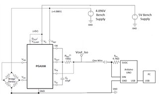
    Can you configure your PGA308 circuit with the XTR116 disconnected as shown in the diagram below? Once this circuit is implemented, please attempt your calibration procedure, then enable Vout and measure the voltage at "Vout_Iso" with a DMM in response to your min and max sensor inputs.


    Once the PGA308 registers are configured and the device is operating as expected, we can revisit the XTR116 portion of the circuit. Note that in the diagram above, the common ground of your voltage supplies is connected to the PGA308 GND pin, the low side of your bridge sensor, and your controller GND pin. Of course, these ground connections will be changed once the XTR116 is implemented back into the circuit.

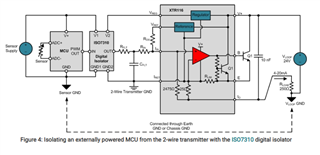
    When the XTR116 is used, your controller must be fully powered between the VREG and IRET pins of the XTR116, and the IRET pin must not be connected to the VLOOP GND or to any other external voltage potentials, including your PC which I believe is connected to the Arduino GND pin through the USB connection. If the Arduino power and GND connections must be tied to your PC, you will need to implement a digital isolator similar to the one shown in this blog post: https://e2e.ti.com/blogs_/archives/b/precisionhub/posts/two-wire-4-20ma-transmitters-background-and-common-issues-part-4 

    Regards,

    Zach

  • Hi Zach, 

    I configured the circuit according to the diagram.

    Here are the corresponding register readings:

    TIFL Register Value: 1100 1100 0000 0000
    
    ZDAC Register Value: 0110 1100 1100 1101
    
    GDAC Register Value: 1000 0100 1100 1101
    
    CFG0 Register Value: 0011 1011 0000 0000
    
    CFG1 Register Value: 0000 0000 0000 0000
    
    CFG2 Register Value: 1000 1000 0000 0000
    
    CHKS Register Value: 0100 1011 0110 0100
    
    CHSR Register Value: 0100 1011 0110 0100
    
    SFTC Register Value: 0000 0001 0000 0000
    
    OENC Register Value: 0000 0000 0000 0000
    
    ALRM Register Value: 0000 0001 0011 1000
    
    OTPS Register Value: 0000 0000 0000 0000

    Here are the corresponding measurements when I attempted the calibration procedure with measured VS = 5.086 V & VEXC = 4.096 V:

    VBR = 0.5 mV, Vout_ISO = 136.5 mV (Vout = 16 mV)

    VBR = 5.1 mV, Vout_ISO = 136.5 mV (Vout = 16 mV)

    As you can see there are faults indicated in the ALRM register & Vout is not changing with change in VBR.

    I do have two questions if you don't mind:

    1) I've been using Decimal # Counts = [(VREF/2 - Zero_DACx_calibrate)*(65536)]/VREF for the ZDAC register.  I noticed from page 89 of the aforementioned TI user guide that Decimal # Counts = [(VREF/2 - Zero DAC RTO VOPGA)*(65536)]/VREF.  What I've been using may not be correct though since page 90 from the same gives Zero DAC RTO VOPGA = (VREF/2 - VZERO_DAC).  The question I have is: does VZERO_DAC = Zero_DACx?  If so doesn't the expression for Decimal # Counts simplify to Zero_DACx*65536 / VREF?  I did try the Decimal # Counts in this fashion but the result is the same behavior as mentioned above.

    2) If operating in Virtual Software Lock Mode, as we are, are 1 wire transactions permitted & reliable during the 1 second delay that occurs just after the CHKS write?  For example, reading from the ALRM register during the 1 second delay?  The output above is with register reads occurring during the 1 second delay.  Trying register reads after the 1 second delay results in CHSR, SFTC, OENC, ALRM & OTPS registers returning zero.

    Thank you!

    Robert

  • Hi Robert,

    The equations on pages 89 and 90 refer to two variables, "Zero DAC RTO Vopga" and "Vzero DAC". "Zero DAC RTO Vopga" is the offset voltage that will occur at the output of the pga due to the zero DAC voltage. "Vzero DAC" is the voltage that occurs at the output of the 16-bit Zero DAC and is internal to the device. As you saw on page 90, Zero DAC RTO Vopga = (Vref/2 - Vzero DAC).

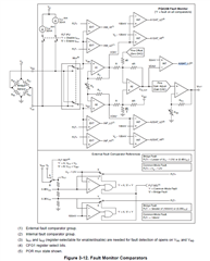
    When operating in Virtual Software Lock Mode, after Vout is disabled and the one-wire is enabled (see figure 5-12), a one-second internal timer is set. Vout remains disabled as long as the PGA308 is addressed with a valid one-wire transaction at least once per second. If the one-second timer is allowed to timeout and the CHSR matches CHKS, Vout is enabled and one-wire communication is no longer possible in your 3-wire configuration. As the output of your PGA is saturated low, you will only be able to read low voltage at the output (in your case 136.5mV) which corresponds to logic zero.

    I see from your ALARM register that internal amplifier A1 is saturated high, A2 is saturated low, and A3 is saturated low. Additionally, [D3] shows that the voltage at VINN is greater than the reference voltage, indicating a bridge fault. Check your bridge sensor connection and ensure the voltages present at Vin2 and Vin1 are as expected. 

    Regards,

    Zach

  • Hi Robert,

    I sent you a friend request on E2E. Once you accept the request we can send messages directly and I can continue to support this issue off of the public forums.

    Thank you,

    Zach