This thread has been locked.

If you have a related question, please click the "Ask a related question" button in the top right corner. The newly created question will be automatically linked to this question.

INA225: wrong gain

Part Number: INA225

Hello Team,

Customer is using INA225 current sense amplifier in one of the design and requested support in clarifying below point. 

 Issue: Need to set the gain of 100V/V by design. But observing more than 300V/V gain in practical.

 20mOhms resistor for current sensing and gain is set to 100V/V.

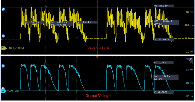
  1. The load current observed is 155mA peak. And based on the calculation design should get 310mV peak as output with 20mOhms current sense resistor and 100V/V gain
  2. But observing 1V at the output of INA225, which seems to be around 322V/V gain.
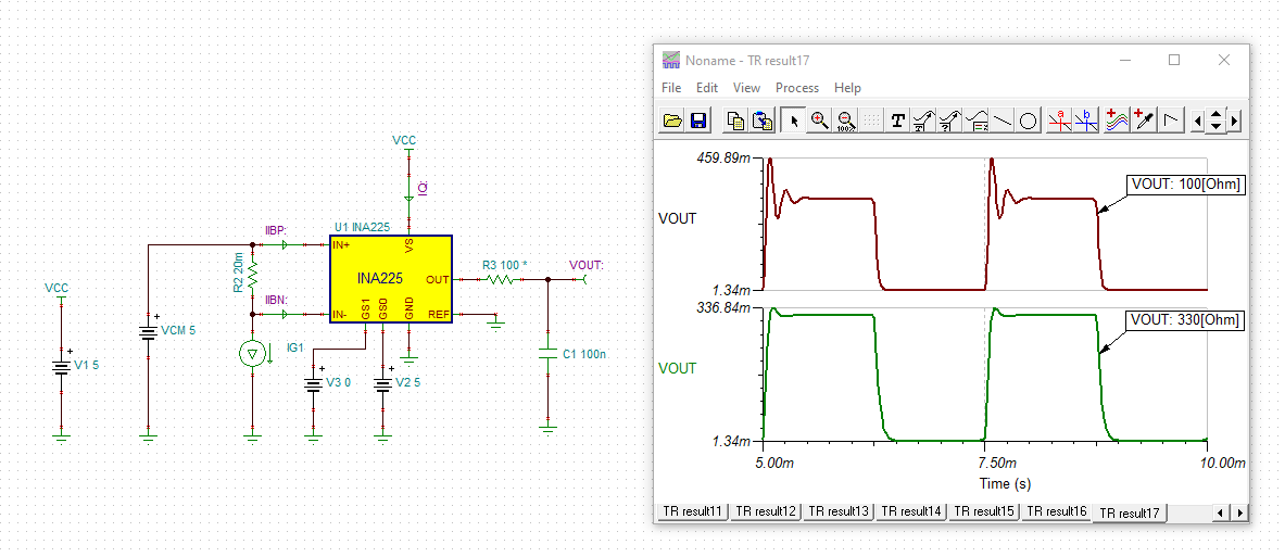
  3. Below is the design, the load current and output voltage waveforms. Request to please review the same and share the possible reason for this mismatch. R81 and R84 are mounted, R82 and R83 are not mounted for gain selection as 100V/V.

Thanks, Shinu.

  • Hi SHinu,

    in any case your R85 = 100R is too small and causes stability issues in combination with the capacitive load of C58 = 100n. Increase R85 at least to 330R:

    shinu_ina225.TSC

    Kai

  • Hello Shinu,

    I agree with Kai as always always.  Please let me know if this does not completely fix the issue.

  • Hi Kai,

    Thanks for the reply.

    Is it really due to the RC at the output? I see below statement in data sheet which is not clear to me.

    With 20 mOhms Rsense what we have, the voltage across Rsense will be less than 10mV. Would that cause the issue?

    The low-offset, zero-drift architecture and precision gain • Programmable Gains: values enable current-sensing with maximum drops – G1 = 25 V/V across the shunt as low as 10 mV of full-scale while – G2 = 50 V/V maintaining very high accuracy measurements over the entire operating temperature range.

    Regards,

    Thomas CN

  • Further, I could see the observed 1.020V at the output is relating closely to 10mV*100V/V gain what I set in design.

  • Hello Thomas,

    The output impedance could be the issue and the ability to drive the capacitive load.  As you increase the series resistor the capacitive load seen that the output is changed at the lower frequency.  

    The statement in the datasheet is just to make you aware with the low Vos and low drift you can still get high accuracy measurements.  

    We have some documentation for the output impedance below.  There is more on the amplifier devices but you have to deal with CSA a little different as they already have a closed loop so I normally don't point to that material to avoid confusion. 

    https://www.ti.com/lit/an/slya029/slya029.pdf

    https://www.ti.com/lit/an/sboa443/sboa443.pdf

    Have you attempted changing the resistor?  Did that fix the issue?

  • Hi Thomas,

    Further, I could see the observed 1.020V at the output is relating closely to 10mV*100V/V gain what I set in design.

    This contradicts with what you are saying in the original post.

    I think all the hassle is coming from the fact that your input signal which far away from being a simple DC signal. Being a heavily changing AC signal in combination with the output ringing due to the instability introduced by the capacitive load makes it impossible to determine the gain of your circuit.

    So, why not runing a DC signal through your shunt? By this you can immediately see whether the gain of your circuit is correct or not.

    Kai