This thread has been locked.

If you have a related question, please click the "Ask a related question" button in the top right corner. The newly created question will be automatically linked to this question.

OPA322: Please review my design and feedback required.

Part Number: OPA322
Other Parts Discussed in Thread: TINA-TI

Hi,

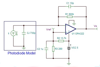
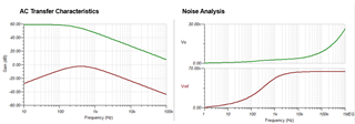
Please see my below design and suggest is there any improvements required.

The photo diode used in this design is MPN : S2386-5K from Hamamatsu.

Will it work properly for very low currents in pA range ?

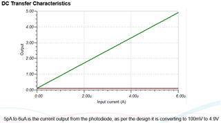
I am calculating the output voltage using :  Vout = (Iin*R1)*Vref.   is this correct ?

 Photodiode.TSC

Regards,

Sebastian

  • Hi Sebastian.

    For the GBW calculation the 10pF is squared, making the calculated GBW quite a bit different than what was calculated. 

    I calculate that the GBW must be greater than 1.5MHz for this application. 

    : 749pF/ {2pi*800k* (10pF)^2} = 1,490,088. 

    The OPA322 will have ample GBW for this application, and the bias current is reasonably low.

    Note, the OPA322 has typical bias current of +-.2pA and a max of +-10pA at 25C :

    It is important to design ample guard band into your design to ensure variation in bias current will not cause problems in your application. 

    The transfer function of the ideal photodiode amplifier is Vout = (Ii*R1) + Vref 

    For example, if your circuit has 2uA flowing through the photodiode, you would have Vout = 1.7V (this matches your DC transfer simulation).

    Yes, this circuit can work well for sensing low currents in the pA range. Understand that process variation and component tolerance will all influence the accuracy of the photodiode amplifier. 

    I recommend leveraging the TINA-TI circuit to evaluate how bias current variation and component tolerance impact sensing performance. 

    Please let me know if you have any questions. 

    Best,

    Jacob

  • Hi Sebastian,

    the circuit is stable Relaxed

    sebastian_opa322.TSC

    Kai

  • HI Kai,

    Thanks for reviewing my design.

    I have on e question, Could you please let me know the function of C5, C6, C7, L2, L3 and C4 in the simulation ? Are they playing any role at the output ? If I go with my exact design(without these additional items at input), will it work like this ?

    Thanks & Regards,

    Sebastian

  • Hi Jacob,

    Thanks for correcting my GBW calculation and your feedback

    Regards,

    Sebastian

  • Hi Sebastian,

    this method is similar to what is shown in the TI's training video series on stability:

    https://training.ti.com/node/1138805

    I introduce a stimulus directly to the input pins of OPAmp and look what comes back via the feedback loop. From the frequency response and phase response I can directly determine the phase margin.

    Because the feedback loop is opened at the input pins, the feedback loop no longer sees the input capacitances of OPAmp ("C5", "C6" and "C7" in the simulation). Because of that the input capacitances have to be "mounted" externally.

    "L2" and "L3" close the feedback loop for DC and allow the OPAmp inputs to be properly DC biased.

    "C4" provides an AC coupling of stimulus without ruining the DC biasing of OPAmp inputs. And because the AC coupling shall be invisible even for the lowest frequencies "L2", "L3" and "C4" are chosen to be "infinitely" high.

    The advantage of this a bit more opulent method is that the complex output impedance of OPAmp is also taken into calculation.

    Kai

  • Thanks Kai


    In my design , can I expect a fully linear output for the input signals from the photodiodes?

    Regards,

    Sebastian

  • Hi Sebastian,

    Yes, this circuit should operate in a linear manner across the input range.

    Please let us know if you have any further questions.

    Best,

    Jacob

  • Thanks Jacob

    I am going through the TI training series which is suggested by Kai.

    Do I need to add any other components to my design ? Please let me know.

    Regards,
    Sebastian
     

  • Hey Sebastian, 

    The TI training series (TIPL) on amplifiers is a great resource for learning about op-amps and circuit design.

    I would recommend adding a decoupling capacitor to the V+ rail, see this post by Art Kay: Decoupling Capacitor

    Otherwise, your circuit looks good to me. 

    When you implement this on a PCB, be sure to keep power traces away from the sensing node. 

    We are always happy to look over layout design if you have any questions on finalizing the design.

    Please let me know if you have any other questions.

    Best,

    Jacob