This thread has been locked.

If you have a related question, please click the "Ask a related question" button in the top right corner. The newly created question will be automatically linked to this question.

LMV7239: LMV7239 output behaviour during power-down.

Part Number: LMV7239
Other Parts Discussed in Thread: TLV1821, TLV1811

I have a design as given attached figure. 

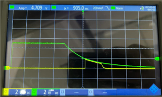
During power down sequence of 5V supply, comparator outputs peak nearly 2V amplitude with ~100msec decaying waveform.

As it is seen in the figure, signal is applied with (+) terminal is 0V level during power down and normally i was expecting 0V logic low output, contrarily.

What could be the reason and more importantly how can i solve this problem?

(i can make a design change if you recommend an adequate solution)

Best regards

İlhan

  • Hi Ilhan,

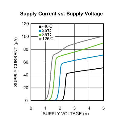
    the LMV7239 is not able to normally work at a supply voltage all the way down to 0V. You can see this from the "supply current vs. supply voltage" figure of datasheet:

    Below a supply voltage of about 2V at 25°C the LMV7239 stops working and the internal circuitry no longer gets properly biased which can be seen from the supply current dropping down to zero. So, for lower supply voltages than 2V the output becomes undetermined.

    Using a comparator with a power-on reset (POR) may be a remedy:

    https://www.ti.com/amplifier-circuit/comparators/products.html#p2192=POR

    Kai

  • Hello Ilhan,

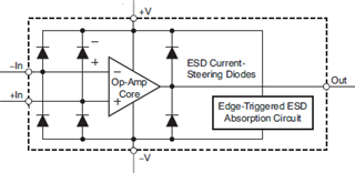
    Normally the output should be high impedance when the supply is zero. But all the pins are ESD diode clamped to the supply pins.

    My guess is that the capacitor is discharging back through the ESD diodes to the supply and output.

    Typical ESD protection:

    You would need to place a resistor between the capacitor junction and the input pin to limit the current, such as 10k. The resistor would be nearly transparent during operation, but would limit the current in shutdown.

    Push-pull outputs have upper ESD diodes on the output. You could also try using a open-drain output device, such as the TLV1821. But the open drain will need a pull-up resistor on the output.

  • Dear Kai,

    Thank you for reply.

    but it seems that internal POR circuitry would not quarantee that i will not come across an enough glitch to trigger load circuit in the comparator output.

    I already noticed that the root cause of this unintented output is the loss of control inside the comparator. And it seems even internal POR would loss the control during power down.

    I need an exact solution because only once trial chance remains.

    Best regards

  • Thank you paul.

    In fact i tried the circuit without capacitor to prevent transparent ESD diode current path but the result was unchanged.

    I think even open-drain structure case, since the external pull-up voltage source would not be instantly zero volt i am afraid i would see somehow similar unintentional pulse that is enough the trigger load circuit.

    Do you have any other recommendations?

    Regards

  • Hello Ilhan,

    I would recommend you use a scope and look at the inputs and output to see what is really happening at power down. What is the power supply power-down ramp rate? What is the input signal? Is it glitching?

    POR does not do much on power-down. All it can do is disable the output when the supply voltage drops below the minimum supply voltage.

    The comparator is still "alive" between 5V and minimum supply voltage. You need to look at the timing of the input signals.

    If you need the comparator to "behave" during power-down, then you may need to isolate the comparator supply voltage so that it still is working while the rest of the system is collapsing. This can be done by placing a (Schottky) diode in series with the comparator supply voltage and adding a large bypass cap to store charge and hold-up the comparator supply for a short period.

  • I will have a look.

    Is there any solution in your mind instead of comparator? For example any analog switch?

    I think the same problem will arise in that case. It seems i need to manage power up/down sequence of the rails. Maybe i can use an open drain comp with a separate pullup rail controlled and damped first.

    What do you think?

    Regards

  • Hello Ilhan,

    First you have to determine if the extraneous output is due to actual input conditions changing, or, due to the comparator operating below it's minimum supply.

    For non-POR devices, the output is not defined when below minimum supply. When ramping below minimum supply, the non-POR device outputs may glitch regardless of the input conditions.

    If possible, yes, you can use an open drain output and connect the pull-up to a controlled voltage, such as the output of a GPIO pin.

    If you must have the output low when the supply is not present, then you could use a JFET to force the output low when the supply drops.

    Again, this all depends on the supply ramp-down rate.

    What is your input signal? Can you provide more details on your application?

  • Dear Paul,

    sorry for late reply, i was out of city.

    Input signal is coming from GPIO pin of 3V3 railed MCU and it is all the way zero during power-down (not monitored in the figure). 

    In the screenshot GREEN is the 5V rail and YELLOW is output of comp. 

    It seems this undesired pulse is due to inherent structure of the LMV7239.

    My aim was to control and level shift the 3V3 level GPIO signal coming from MCU to 5V logic with additonal COMP.

    Regards 

  • Hi ilhan,

    Yes you're right  For our older devices, the output is not defined when operating below the minimum supply voltage as we can see the glitch occurring. I think if you could use a POR device such as the TLV1811/TLV1821 as these have defined output levels below the minimum supply voltage. See here: [FAQ] How Power on Reset Comparators Simplify Designs - Amplifiers forum - Amplifiers - TI E2E support forums.

  • Hi Ilhan,

    the crucial question is here: Why at all must the comparator work when the +5V supply is decaying? Why is a malfunction at a supply voltage of +2V not tolerable? How are the +3.3V supply and +5V supply related to each other?

    The next crucial question is: Down to what supply voltage must the comparator properly work?

    And the third crucial question is: How must the comparator work when the supply voltage is decaying? Must a low input signal give a low output signal and a high input signal give a high output signal? Or must only give a low input signal a low output signal and a high input signal is allowed to be suppressed to zero?

    So, Ilhan, please elaborate all these relevant details so that we can find a remedy.

    Also, how speedy are the signals that must be level shifted? Must a fast comparator be used at this point?

    Please give as exact details as you can.

    Kai

  • thanks Kai, these are good questions to ask

  • Dear kai

    Thank you for questions i could reply are;

    #Why at all must the comparator work when the +5V supply is decaying? Why is a malfunction at a supply voltage of +2V not tolerable? How are the +3.3V supply and +5V supply related to each other?

    <>The output of comparator drives a low-side FET that normally initiates a solenoid for emergency activity. By mistake it alerts the system as if an emergency state arises.

    #Down to what supply voltage must the comparator properly work?

    <>According to input pins states the comparator output normally should be at zero level irrespective of supply level. Pls have a look once again the scope screenshot. While output is zero comparator unintentionally gives a peak that is enough to drive connected FET to alert the system erronously.

    #How must the comparator work when the supply voltage is decaying? Must a low input signal give a low output signal and a high input signal give a high output signal? Or must only give a low input signal a low output signal and a high input signal is allowed to be suppressed to zero?

    <>(-) input is connected to 5V supply with 10K+10K resistor divider and is set to 2.5V, (+) iput is driven LOW level by MCU and the expected output is ZERO volt at the output. In summary i have to eliminate this ~200msec unintentional pulse.

    I will try the same circuit with a Comparator including internal POR. It seems there is no any other way.

    Regards

  • Dear Chi,

    I had a look at the link you sent.

    But i could not find the below figure in the relevant datasheets?

    Regards

  • Hi ilhan, which datasheet or which devices are you looking at? TLV1811, for example, POR is discussed in section 8.4.3

  • Hi Ilhan,

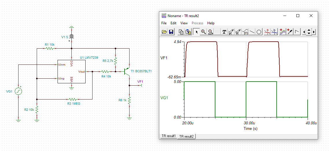
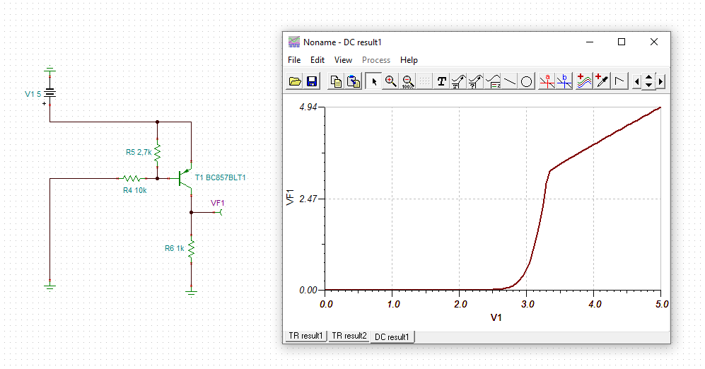
    this circuit can eventualy do the trick:

    Ilhan_lmv7239.TSC

    Kai

  • Thanks Kai, thats a neat circuit.

  • Dear Kai,

    Thank you for your recommended circuit.

    I will test this modification.

    Best regards