This thread has been locked.

If you have a related question, please click the "Ask a related question" button in the top right corner. The newly created question will be automatically linked to this question.

INA229: Where do I get the ground in the low-side, bidirectional current sense amplifier?

Part Number: INA229
Other Parts Discussed in Thread: TIDA-00302

Hi all,

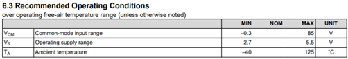
I'm going to use the INA229 as lithium battery power monitor in low-side style but I'm worried about the low common mode input range of the pin IN+ and IN-.

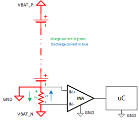
In a situation like this I have two cases:

  • Charge (green): the IN- pin of the INA could reach a negative voltage of -163.84 mV (max ). The Vin(CommonMode)=(-163.84+0)/2=-81.92 mV
  • Discharge (blue): the IN- pin of the INA could reach a positive voltage of +163.84 mV (max ). The Vin(CommonMode)=(163.84-0)/2=81.92 mV

I'm worried due to the negative voltage of the IN- pin. The common mode input voltage is still in the ABS ratings but is very close to -0.3V.

Is this the correct way to use the INA229 ?

Thanks

  • Hello Luca,

    I'm worried due to the negative voltage of the IN- pin.

    The ABS max ratings are the right place to look for survivability, but you should also look at the recommended operating conditions: 

    For this device Vcm remains the same at -0.3V for the operating conditions. Keep in mind each pin individually, not the average of the two, must stay within the Vcm ABS max ratings, so for example you can't have one pin at -0.4V and the other at GND without risking device failure.

    For your application, a negative voltage of -163.84 mV should be fine, but you should be aware of any transients/noise or current spikes in your system as they may cause the voltage to exceed the ABS max ratings.

    Is this the correct way to use the INA229?

    I'm confused about the extra ground you have at the IN+ pin. If you have another path to ground outside of the shunt I'm concerned that current will not be measured properly because some of the current will be diverted to ground. If you ground the VBAT_N/IN- node instead of IN+ it would solve this problem.

    You could also use the INA229 on the high side if it is less than 85V.

    Levi DeVries

  • Hello Levi,

    thank you for your reply.

    I'm confused about the extra ground you have at the IN+ pin. If you have another path to ground outside of the shunt I'm concerned that current will not be measured properly because some of the current will be diverted to ground. If you ground the VBAT_N/IN- node instead of IN+ it would solve this problem.

    Yes, you're right. It's best to use the VBAT_N node as GND. I modified the schematic as you suggest:

    Now I'm in trouble with the spikes/surges/EFT that can occours and may cause the voltage to exceed the ABS max ratings. By reading the AN TIDA-00302, I think the previous circuit to will solve the EMC issue in the following way:

    R1, R3 and the TVSs are there to dissapate the high amount of energy of the spikes; the ferrites FB1 and FB2 are useful for fast transient (mainly the EFT) and the resistors R2, R4 and the diodes D1 and D2 (probably shottky diodes with Vf<0.3V) clamp the residual voltage to 0.3V.

    Any other ideas or improvements of the previous circuits?

    I cannot uses the INA229 in high-side because of the voltage of the batery that could be > 85V.

    Thanks

  • Luca,

    The TIDA-00302 document is good to reference for this application, be sure to take a look at the INA229 datasheet notes for filtering and dealing with transients as well: 

    Something to note is the maximum values for the series resistance (100Ω), as exceeding these values will reduce the accuracy of the device. The INA229 has a lower input bias current than the devices in the TIDA-00302 document, so it will have a slightly higher limitation on the series resistance. I would also recommend staying within the suggested capacitance values (0.1-1µF).

    Let me know if you have any more questions,

    Levi DeVries