This thread has been locked.

If you have a related question, please click the "Ask a related question" button in the top right corner. The newly created question will be automatically linked to this question.

PGA 280 Help

Other Parts Discussed in Thread: ADS1259, PGA280, ADCPRO, INA117, PGA204

Hi,

I am facing a problem with PGA 280 on the evaluation board of ADS 1259. I am giving the following power supplies to PGA 280.

VSP, VSN = +/- 15v w.r.t Ground

VSOP,VSON = +/- 2.5v w.r.t Ground

DVDD,DGND = 3.3v w.r.t Ground

VOCM pin is connected to ground where Ground is common to all and is the midpoint of +2.5 to -2.5V (VSOP to VSON).

The gain is set to 1/8 and the input given is 4v. Ideally I should get 0.5v as the output. However the output is seen fluctuating beween 630 to 640 milli volts. When i checed the VON pin w.r.t Ground, it gives a stable 0.250v. However VOP w.r.t Ground shows fluctuation of around 380 to 400 millivolts. This condition has been observed earlier. I need to know the reason behind such fluctuations. Please reply at the earliest.


Regards

Rahul

  • Hello Rahul,

    I have set up the ADS1259+PGA280EVM-PDK.  I have set up the device with the following voltages:

    MMB0 supplies: +/-15V; these are connected to J14, VA+/VA- on the MMB0 board; verified at  the ADS1259EVM/PDK at J11 pins 1 and 2 (VSP,VSN)

     +/-2.5V supplies connected  directly to J10  pin 2 and pin 4 (AVDD/AVSS) of ADS1259/PGA280EVM board

    DVDD is 3.3V.  All the voltage supplies have the GND/COM connected together.  The gain is set to 1/8.

    I have connected a  DC 4V signal generated using a Data Precision analogic and is connected to IIN1 and INP1 of J8 on the ADS1259/PGA280EVM.  the INN1 is also connected to AGND (J8-19) on the ADS1259/PGA280 EVM.

    I have measured the output VOP/VON to be the expected +/-0.250V with respect to GND (TP6) or 0.5V across VOP/VON.  VOCM is set to the middle of supplies by placing S3 at the middle position (using the voltage divider R8/R9 on the EVM).  I also repeated the experiment by setting S3 to J8 pin 17 VCOM; and shorting VCOM to AGND (J8-19) and obtained the same results.

    I need to ask  a few questions to ensure I understand your set up:  How is the 4V DC input signal generated or what source is being used? Is the input signal referred to AGND (J8-19 or TP6)? How are the supplies being Grounded? How exactly is VOCM set to GND or what is the position of switch S3 on the ADS1259/PGA280 EVM? Is there any noise/oscillation on the input signal?

    Thank you and Regards,

    Luis 


  • Hi Luis,

    Barring a few changes, I have exactly the same setup that you have described.

    The changes are as follows:

    1. The i/p given to PGA through INN1 and INP1 is purely differential i.e the INN1 pin is not connected to AGND.

    2. I have connected capacitors C20, C21 and C22 to AGND instead of AVSS.


    Luis Chioye said:
    How is the 4V DC input signal generated or what source is being used? Is the input signal referred to AGND (J8-19 or TP6)?

    Answer: The 4V DC i/p is generated using a calibrator to give accurate inputs to the PGA. No the input signal is not reffered to AGND(J8-19 or TP6). The voltage is measured  w.r.t each other i.e TP14 w.r.t TP13.

    Luis Chioye said:
    How are the supplies being Grounded?

     Answer: I have used two power supplies to generate +/- 2.5V , +/-15 V and external reference 1.25v for ADC. All the grounds of these voltages are made common to the board ground. I.e TP6 (GND).

    Luis Chioye said:
    How exactly is VOCM set to GND or what is the position of switch S3 on the ADS1259/PGA280 EVM?


    Answer. The switch is S3 is connected to HDR which gets connected to connector J8. I have shorted pin 15 and 17 of J8.(VOCM is shorted to AGND)

    Luis Chioye said:
    Is there any noise/oscillation on the input signal?

    Answer: No there is no appreciable noise in the i/p signal from calibrator.


    My observations:

    After i connected the internal switch of PGA C1 or G1 to VSON then the o/ps became stable. i.e the voltages above and below VOCM did not fluctuate.


    Regards

    Rahul

  • Hello Rahul,

    The input stage of the PGA280 can accept differential or single ended signals.  The restriction is that both positive and negative inputs must stay between the VSN and VSP voltage supply potential. 

    The allowed voltage range Is:

    VSN +2.5V < Input Voltage Range < VSP - 2.5V; or in our example -12.5V < Input Voltage Range < +12.5V

    When enabling C1, the negative input is attached to -2.5V; so INN1 = -2.5V and INP1= +1.5V; so both inputs are inside the -12.5V to +12.5V range.

    Could you please repeat your experiment and while applying the 4V differential signal, connect one of the inputs to a fixed voltage? The key is that this fixed voltage must be referred to the same GND and both inputs must be inside the input voltage range.  For example you could try connecting INN=GND, or INN to VSOP, or INN to a fixed voltage between -12.5V to about +8.5V.   One possibility is that the generated differential signal of 4V coming out of the calibrator is outside the allowed range since the differential signal is being allowed to float.  Please let me know if this solves the issue.

    Thank you and Kind Regards,

    Luis


  • Hi Luis,

    I did the experiment you told me to do.

    When INN1 is connected to ground then the o/p voltage becomes stable.At 4 volts it shows 0.125v above and below GND. Also the input voltage to PGA is well within range. However my requirement is a pure differential input voltage to be given to PGA. But when i remove the ground...then the o/ps start fluctuating again i.e only the VSOP w.r.t VOCM. Please suggest a solution over this.


    Regards

    Rahul

  • Hi Rahul,

    In order to make a suggestion, I need to ask you more questions about the input signal.   

    What type of device or sensor is providing the input signal?

    What is the common-mode voltage range expected at the inputs of the amplifier (Common mode Voltage = (INP+INN)/2 ) with respect to GND?

    What range of differential voltage signals are to be expected?  Are these DC signals or what frequency range of signals are to be measured?

    The PGA280 is an instrumentation amplifer and requires the inputs to be inside the range of the input stage supplies.

    Thank you and Kind Regards,

    Luis


  • Hi Luis,


    The input signal is going to be +/- 10v differential. There is not going to be a common mode input to PGA. The frequency of the input signal will be lesser than the slew rate of PGA. A DC signal is also expected at the input.

    Well I wanted to ask you one more question. Even if we assume noise at the output of calibrator, why is it that the voltage at VSON w.r.t VOCM does not fluctuate at all and only the voltage VSOP w.r.t VOCM fluctuates. I mean can you please explain under which conditions can one of the o/p w.r.t VOCM(i.e either VSOP or VSON) fluctuate, apart from the inputs to PGA being noisy or unstable?


    Regards

    Rahul

  • Hi Rahul,

    I have tried to reproduce the problem using the test conditions described on the post and the output VOP-VON is still stable at 0.5V.  I also performed different combinations where I performed a sweep of the input common-mode voltage while holding the differential voltage constant at 4V. Provided that both positive and negative inputs where inside the input voltage range; the reading was stable.

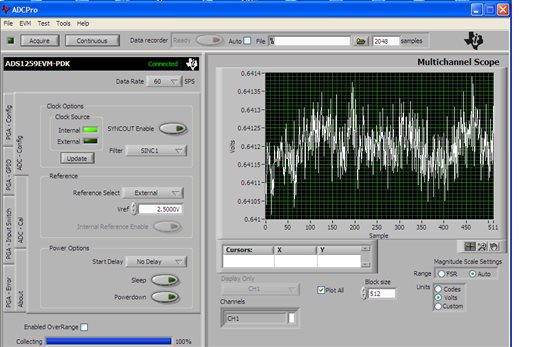
    I was able to obtain unstable readings only if I left the 4V differential signal floating; where readings were fluctuating, obtaining a similar behaviour as you described (sometimes).  If I forced on purpose INN << -12.50V with respect to AGND; or  INP>>12.5V putting the device outside of range;  I obtained unstable readings. (about ~0.640V for the INN=-14.5V case.

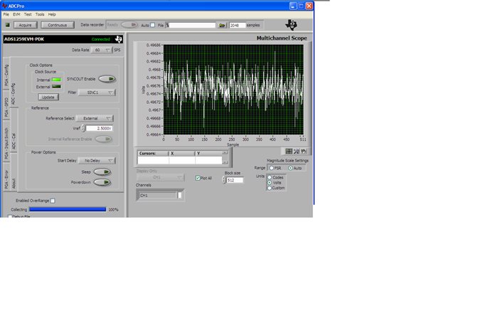
    It may be possible that in the set-up a ground loop may be formed; where one of the supplies is not at the expected voltage.  Please see ADCPro plots below.

    If you can provide a diagram/schematic of how the supplies are being connected; and/or DC coupled oscilloscope plots of the input signal (both negative input and positive input) with respect to AGND this could help. 

    Regards,

    Luis


    VOP-VON plot; G=1/8; INP1 - INN1 = 4V; INN = -12.5V to 8.5V with respect to AGND; Readings Stable 

    VOP-VON plot; G=1/8; INP1 - INN1 = 4V; INN = -14.5 with respect to AGND;Measurement unstable(outside input range) 

    add 

  • Thanks for your replies.

    Luis Chioye said:

    It may be possible that in the set-up a ground loop may be formed; where one of the supplies is not at the expected voltage.  Please see ADCPro plots below.

    I am going to check this out. Also we have strict requirement of diffrential input voltage. So i have never tried with a common mode voltage except when you told me to do so in the earlier posts.


    Luis Chioye said:
    I was able to obtain unstable readings only if I left the 4V differential signal floating; where readings were fluctuating, obtaining a similar behaviour as you described (sometimes

    Please can you explain a little bit more. Isnt diffrential signal always floating? According to my existing setup, the grounds of all the supplies for PGA and ADS are the same.The differentail signal is produced by the calibrator whose ground and the board goround have no relation at all. I will upload the block diagran as soon as possible.


    Regards

    Rahul

  • Hi Luis,

    I want to share another observation with you. I am using a digital voltmeter to measure the input and output voltages. Now the voltmeter can show a reading upto three decimal(for eg: 0.000 or 1.000) upto 2 volts. I gave the input to the PGA from the calibrator and set it to 2.000v, and i measure it at the input terminal of PGA (INN1 and INP1).It does not show any  fluctuations at all on the voltmeter. Now i use the same voltmeter to measure the o/p voltage i.e VSOP w.r.t GND and  VSON w.r.t GND.I have kept gain at 1/8. Now VSOP is seen fluctuating from 0.350v to 0.355v w.r.t GND and VSON is seen constant at 0.125v. These are the readings as shown on the meter. Now even if the calibrator is inducing some noise on the input lines to PGA, the voltmeter is not measuring it because the amplitude is not enough for voltmeter to detect changes(shows constant at 2.000v and i held it there for 30 secs atleast).However the same voltmeter shows fluctuation in millivolts on the o/p of PGA..The voltmetershould not be measuring any fluctuations at the output. Again VSP and VSN are at +/- 15 v, VSOP and VSON at =/- 2.5 v(All the voltages are same as described in the first post, none of them have been changed). The i/p differential voltage to PGA  is at 2.000v which is well within the limits. In such conditions can you please explain the behaviour of PGA?. Here we can eliminate any errors caused in measuring and also the noise contribution to the input of PGA.This observation is the same as before but i have given more details this time.

    Regards

    Rahul

  • Hi Rahul,

    Thank you for looking into this and providing the voltage supply information.  When designers work with linear amplifiers such as instrumentation amplifiers, op-amps, digital programmable gain amplifiers, and difference amplifiers, they must always consider both the differential input voltage range, and the common-mode range or input voltage range of the signal input source with respect to the supplies of the amplifier. This is not always an easy or trivial problem.  Instrumentation amplifiers have generally an input voltage range requirement with respect to their supplies.  Other amplifiers, such as difference amplifiers may have a common-mode range signal requirement that can be above their supplies; for example the INA117 has a common-mode voltage range of +/-200V that can be above its voltage supplies +/-15V. 

    Some amplifiers specify this input voltage range in terms of the common-mode voltage, where common mode voltage is the average voltage of the inputs (INN+INP)/2. In the case of the PGA280, the input voltage range is simply specified as the input voltage with respect to its input supplies.  In the PGA280 is required that both inputs voltage potential are inside the range:

    (VSN) + 2.5V < INPUT Voltage < (VSP)-2.5V; where the Input Voltage is the voltage of IN+ input or the IN- input with respect to the VSN and VSP supplies. 

    In our case, the voltage supplies are VSN =-15V; and VSP=+15V. Therefore the input range limits are:  -12.5V < INPUT Voltage <+12.5V.  Let's say for example, INN=-15V and INP=-11 giving 4V differential.  This voltage is outside the linear range of the device since INN is outside the -12.5 voltage limit above.  Another example, INN= 3V and INP = 7V; the differential voltage is still 4V but this time both inputs are inside the linear range of the amplifier.   

    One classical application of instrumentation amplifiers is to connect a sensor; such as a thermocouple to an instrumentation amplifier.  The thermocouple provides a differential signal that will vary a few +/- ~100 mV in range.  The user must set or fix the input voltage of this thermocouple in the linear region of the Instrumentation amplifier. I borrowed the following section from the PGA204 datasheet which is a different instrumentation amplifier device; with a different set of common-mode requirements, however the concept of common-mode voltage is still valid.  Please see example of different sensors with different circuit setting the common mode below.


    These circuits above have a well defined potential with respect to the voltage supplies of the instrumentation amplifier.  Note: The differential signal does not have to be directly connected to GND; however it must have a well defined potential with respect to the instrumentation amplifier supplies. For example, in the thermocouple circuit above, you could have the thermocouple's 10Kohm resistor connected to +3V with respect to AGND and be in the linear range; since both inputs of the PGA still are inside linear region; the thermocouple provides a differential signal of +/-`100mV...

    In your example, the calibrator is providing a fixed 4V differential between INN and INP; however, if the user only connects this differential voltage and does not provide a way to define the input voltage with respect to the  to the VSN and VSP supplies;  the 4V differential voltage will "drift" freely or "float" between the input analog supplies  VSP and VSN; and most likely in this case the signal can drift such one of the inputs its only being held by the internal protective clamp (ESD diode) of the instrumentation amplifier. When this happens the amplifier is already outside of its linear region. 

    In any application, it is essential for the designer to know in advance the expected common-mode voltage of the input signal source generating the differential signal or provide a circuit that will establish the input voltage with respect to the input analog supplies.  I understand you have already mentioned that in your application your signal does not share a GND point with respect to the PGA, however, it is necessary to understand how much above or below this voltage is to be expected with respect to the amplifier supplies in order to select the appropiate device/solution.

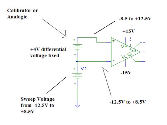
    In our case, I tested the PGA280 with the following circuit:


    This circuit provides a well defined voltage for the inputs of the amplifier with respect to its VSN and VSP supplies.

    Hope this helps,

    Luis


  • Hi Luis,

    I think i have been a little ignorant to your suggestion of the input voltage to be within range of VSN and VSP. Also thanks for the detailed explanation that you have given so far.

    Ok, so you want to say that although calibrator is giving a differential output signal but the voltage w.r.t VSP and VSN is not within the limits and that is the reason why the non linear or fluctuating behaviour at the output of PGA. In that case I will check the voltage between INN1 w.r.t VSN and INP1 w.r.t VSP. These voltages should be between +12.5 and -12.5 volts. Also please can you suggest a scheme to keep the differential input voltage within limits? I can think of adding a 1 megaohm resistor between both the input terminals and GND.  Kindly provide me with your email so that I can share a part of our input circuit with you.My email address is rahulnadgouda@gmail.com


    Regards

    Rahul

  • Hello Rahul,

    Thank you very much.  I will follow up with the questions directly via email

    Regards,

    Luis

  • Hi Luis,

    I apologize for taking so long to reply to your post sice I was caught up with some other work. Well you had told me to reference the i/p of PGA w.r.t board ground so that they dont go out of specified range (VSP - 2.5v to VSN + 2.5v) and hence i wont get any non linear behaviour at the o/p of PGA. I did come across one condition where i did not reference the PGA i/p w.r.t board ground, i.e i left them floating and gave an 8 v differential signal from the calibrator. The gain was 1/8 so ideally the PGA should give 1 v at o/p. However i experienced the non linear behaviour which i mentioned earlier. I checked the voltages and the i/p to the PGA w.r.t board ground were well within range.So in that case why did the PGA show the non linear behaviour?.


    Regards

    Rahul

  • Hi Rahul,

    When you are measuring the voltages are you using a regular multimeter? Many voltmeters have a finite input impedance of about ~10MOhm. One possibility is that the ~10MOhm input impedance of the voltmeter is pulling the inputs into range since you are basically placing a resistor between the PGA input and GND when connecting the voltage meter to perform the measurements.  If you leave the voltmeter connected at the inputs to GND, is the voltage on the PGA still unstable?

    Essentially the inputs of the PGA280 must not be left floating.

    Best Regards,

    Luis

  • Hi Luis,


    Yes I agree to your point that a 1 Meg resistor inside the multimeter could be pulling one of the input to ground. I will carry out the experiment again and connect another voltmeter at the o/p of PGA to see whether the o/ps fluctuate. If the o/p does not fluctuate then this concludes the issue. I will have to carry out the experiment on Monday. Till then please can you explain me the input switch structure of the PGA with an example because in the datasheet nothing has been explained in details.


    Regards

    Rahul

  • Hi Luis,

    I conducted the experiment like you told me to. When i connect the voltmeter between one of the i/p of PGA and board ground and another voltmeter between the o/ps of PGA, then the o/ps stop fluctuating.Hence this concludes the issue. I have added a 1 Meg Ohm resistor between both the PGA i/ps and board ground. Is there any other method that you would like to suggest? Also i have a few queries regarding the ADC. Do you want me start a new thread or continue in this one? I appreciate your efforts you have put in by explaining me the details. Thank you very much.


    Regards

    Rahul

  • Hello Rahul,

    That's good news.  Depending on which type of sensor or source is generating the signal; placing a 1MOhm from the inputs to GND may work fine.  In some cases, I have also seen users place a 1MOhm resistor from the VSN pin to INN and from the VSP pin to INP.

     Yes, if you have more questions related to the ADC please start a new thread on the Precision Data Converters forum (or contact via e-mail).

    Thank you and Kind Regards,

    Luis

  • Thank you Luis, I have added 10 Megs resistors.Thanks for your help.