This thread has been locked.

If you have a related question, please click the "Ask a related question" button in the top right corner. The newly created question will be automatically linked to this question.

INA1620: Stability analysis

Part Number: INA1620

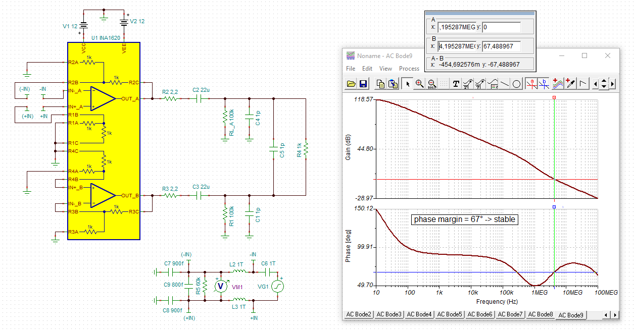
I started with an example model using TI TINA with the INA1620, and modified it for circuits that we are considering for driving the reference for a couple of different resolvers.  I am primarily interested in the stability of the circuit with various discrete component configurations as loads on the output(s).  Some of this is also for my education on the TI TINA tool and how to do stability analysis on various circuits.

Initially I tried to replicate the results of the author, but the Bode Plot is hard to replicate without knowing exactly what the graphs mean.  Is the original Bode Plot, the open circuit analysis of a single complete differential amplifier as shown?  I was thinking that the inverting and non-inverting portions would have to be analyzed separately, as they would each of different gain-phase margins.  Any help on how the original analysis was done and on how to person a stability analysis of our modified circuit would be appreciated sbomal5a_L_ACB_A1.TSC

  • Conrad,

    Regarding the original stability analysis.  I assume that you are referring to this document:  slyt630.  Correct?  I am looking at this circuit now.  If you mean something different by the original analysis, please let me know specifically which document and section you are referring to.

    Art

  • Hi Conrad,

    I would do the phase stability analysis this way:

    conrad_ina1620.TSC

    Kai

  • Thanks Kai,  That is really helpful.

    Conrad, Let us know if that solves your questions.

    Art

  • The example of how to separate the DC bias from the AC analysis is very helpful.  This allowed me to do most of the analysis that I wanted to do.

    I am still confused by the Datasheet, sheet 10 "Figure 24. Phase Margin vs Capacitive Load", where the Phase Margin is different if the amplifier configuration is "G=+1" vs G=-1".  The AC analysis seems like it would be indifferent whether the topology in inverting of non-inverting?  Any explanation of this graph and how it applies to using the part would be appreciated.  Obviously, the capacitive loading affect shown for "G=-1" would be preferred.

  • Hi Conrad,

    the gains 1V/V and -1V/V not only differ by the sign but also differ in the associated noise gains: A gain of 1V/V means a noise gain of 1V/V, but a gain of -1V/V means a noise gain of 2V/V, which makes a big difference when it comes to stability. Because of that an OPamp running at a of gain -1V/V usually tolerates a higher load capacitance.

    Kai

  • Hi Kai,

    Would it be possible to show, using the TINA spice with INA1620, the different capacitance stabilities?  From my understanding the topology is the same for G=+1 and G=-1 (just the forcing function is different), and therefore the open loop gain equation is the same, whether the external input (i.e., forcing function) is fed into the +terminal of the Op-Amp or into a resistor connected to the -terminal of the Op-Amp.  I.e., my simulations are the same whether I am using as inverting or non-inverting Op-Amp; I can't even see how I would set up the simulations differently ;-/.

    Conrad

  • Hi Conrad,

    I would do it this way:

    Kai