Other Parts Discussed in Thread: LMP2021, OPA391, OPA396, OPA392, OPA325, TLV387, OPA387
Hi Team,
My customer uses OPA376 as differential amplifier to sample DC current.
Customer finds that the output of OPA376 drops a lot when temperature rises to >90℃, and the drop voltage is different when using different OPA376. For example, in 25℃, the output is about 2V, but in 90℃, some amplifier’s output drops to 1V, the others may drop to even 0.1V. (the voltage drop is too large so I think it should not be caused by temperature drift)
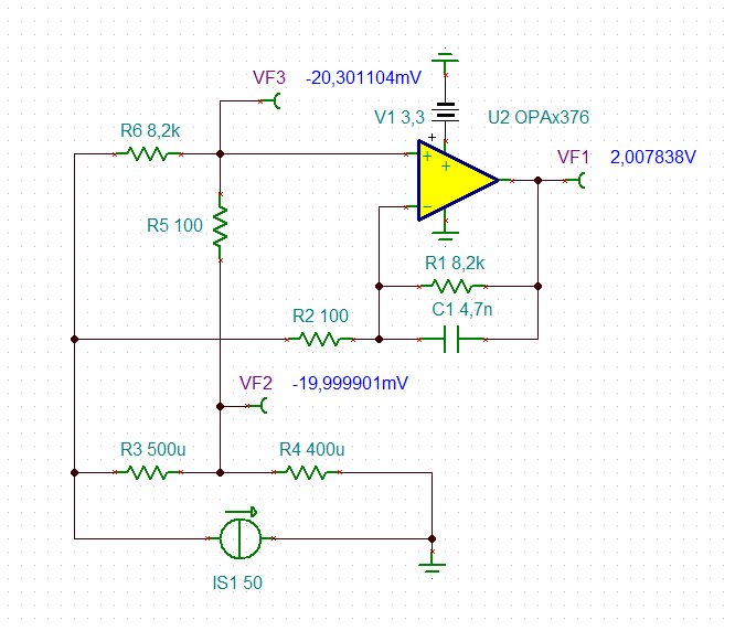
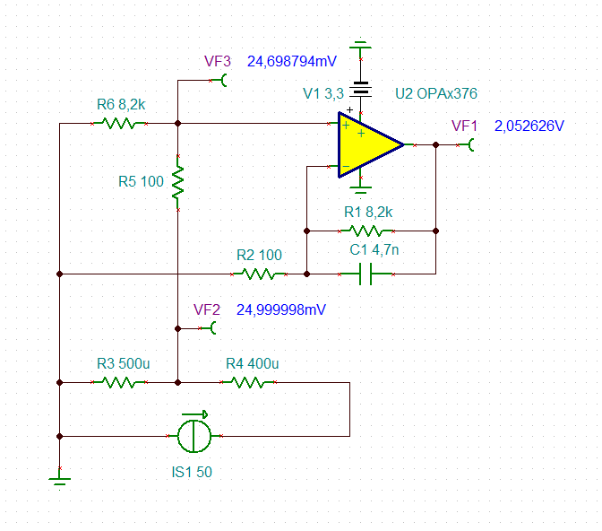
Here is the schematic.
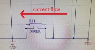
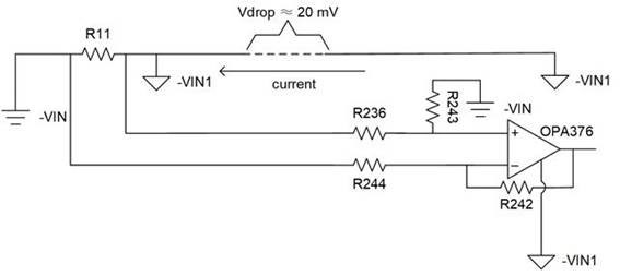
The left one (R11) is sensing resistor, 0.5mΩ. The DC current is about ~50A.
The right one is differential amplifier, R236 = R244 = 100 Ω, R243 = R242 = 8.2 kΩ, C208 = 4.7 nF
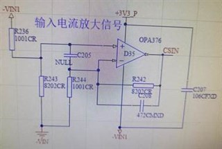
One thing needed to be noted is that because of long routing of -VIN1, so there is extra voltage drop here, it is about ~20mV.
So here are the questions:
- Customer wants to know why OPA376 can’t work normally in this condition.
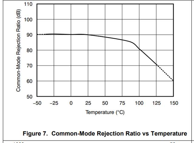
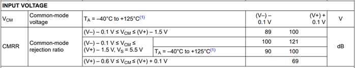
- Personally I think it may be related to common-mode input range, because the negative input voltage is lower than reference ground of OPA376, and there is an extra voltage drop of positive input. But in d/s, I only find the common-mode voltage range in 25C, could it become very low when temperature rising?
And more, customer also try with LMP2021 and find it can work in 90C without any voltage drop. I find the common-mode voltage range of LMP2021 is larger than OPA376.
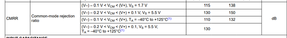
LMP2021:

OPA376:

Let me know if you need more information. Thanks.
Regards,
Nathan