This thread has been locked.

If you have a related question, please click the "Ask a related question" button in the top right corner. The newly created question will be automatically linked to this question.

INA293: Questions concerning INA293 commissioning

Part Number: INA293

Hallo together    ,


we are planning a design with the INA293B1, where we want to measure a shunt current and want to detect a short-circuit current.


To detect the short-circuit current as fast as possible we need the full slew rate of the INA293 with 2,5V/µs as described in the datasheet.


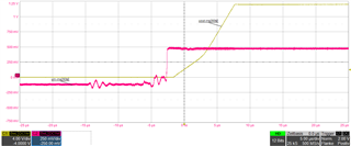
In a first test (VCC=19V, CVCC=100nF, Ta=25°C, INA293B2, Output: Probe 10:1, 10pF) with an input ramp of 0,5 V to the plus-input when minus-input is connected to GND shows a delay of approx. 1,25µs until the

INA293 reacts concerning the input voltage. (You can see this behavior in the appendix „slew-rate-ina293.png“)


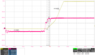
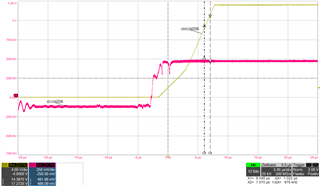
What we saw else is the varying slew rate starting from around 1,3V/µs (half of slew rate in datasheet and coming up to 3V/µs)

See „picture slew-rate-ina293--00001.png“ and „slew-rate-ina293--00005.png“


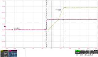
Concerning Table 7-2 Response time from the datasheet the response time at Vin= 0,3V in our case should be (0,3V*50V/V)/2,5V/µs=6µs.


In our case we have got 9µs. „slew-rate-ina293--00006.png“


Questions:


  • What is the reason for the first delay?
  • What is the reason for the two different slew rates?
  • What are the reasons for the difference between measured response time and calculated response time/response time from datasheet?
  • Hello Patrick,

    For the first delay is normally when you start you have a voltage at or below zero to start or a point where the output is saturated.  I am not sure if that is exactly the case as I cannot tell the zero for the INA293B1 output( I assume it is zero output at beginning) .  With the output saturated (input at 0V) the device will take some time to recover.  You could see some variation from device to device as the offset could be positive or negative on the device.  This causes both the prop delay and the slower slew rate.  Getting out of this saturated output condition cases the input to slew slower until it recover completely on some internal nodes.  This is the cause of the two slew rates you are seeing.  The datasheet as the input larger at the start. 

    The fix for this if you can deal with a little gain error and offset error is to add a resistor in series with one of the inputs as this will cause a positive offset.  20µA * 10Ω= 200uV input offset.  The gain error from this will change as the IB changes with Vsense.  If you place it on the IN+ pin the gain will increase, If you place it on IN- then the gain will decrease.  An example is at 10Ω * -120µA*20V/V = 24mV error at output (120µA @900mV input Vsense Figure 6-15 in datasheet) 24mV/900mV*100 = 2.66% error.

    Regards,

    Javier