This thread has been locked.

If you have a related question, please click the "Ask a related question" button in the top right corner. The newly created question will be automatically linked to this question.

XTR111: 100°C operation

Part Number: XTR111

Hi,

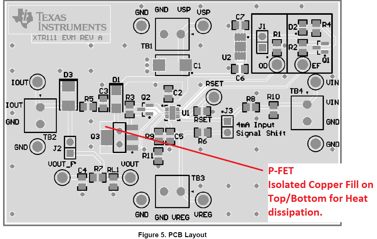
In datasheet is written that work temperature range for XTR111 is - 40 - 125 °C. My Customer has a problem  with temperature upper limit. There is a quite large difference in output current compared to the result for 100 °C (it is around 7%), is this something unusual? Load Resistance 50 and 500 Ohm at the output of the circuit and the worst case is for 50 Ohm resistance.

Thank you,

Daria

  • Hi Daria,

    this can happen when the current relief p-MOSFET isnt sufficiently thermally isolated from the XTR111 and begins to unwantedly heat up the XTR111. As a remedy, allow the p-MOSFET to be properly cooled by a enough "copper" on the printed circuit board. Remember that the p-MOSFET needs a local, isolated copper plane on the solder side of PCB as a heat sink. Also, have enough distance between the XTR111 and the p-MOSFET. The

    XTR111 Evaluation Module User's Guide (Rev. B)

    shows a nice and proven layout example.

    Kai

  • HI Daria,

    I agree with Kai.  If you would like us to review the schematic and PCB board layout please let us know.  

     You may also want to ensure the thermal pad of the XTR111 is connected to the GND,  The leadframe die pad should be soldered to a thermal pad on the PCB.

    The heatsink of the P-FET transistor is often the main culprit when issues at hot temperature occur. The dominant portion of power dissipation for the current output is in the external FET. It is important to consider the power dissipated by the external FET, which is a function of the power supply voltage, and current output range.    

    Please include the appropriate heatsink for the FET in the design.  For example, the XTR111-2EVM incorporates the ZXMP6A13FTA P-Channer MOSFET on the SOT23-3 package. If you refer to the XTR111 board layout on page 7 of the XTR111EVM User's Guide, the drain of the P-FET (pin2, pin4 heat sink) are connected to an isolated copper fill on Top and connected to another isolated copper fill on the bottom for heat dissipation.

    Thank you and Best Regards,

    Luis

  • Hi Luis,

    Sorry for the late reply,

    The customer desoldered the bipolar transistor from the circuit, and that made a large difference. Now they have less than 1% measurement error.

    I would like to ask if is it necessary to have this transistor in circuit? I have attached schematic with XTR111 (there is still bipolar transistor).
    The behavior from Evaluation Board is quite similar, and that is why they asked about upper temperature limit – if there is normally noticeable difference for 125 celsius degrees, or something creates this large error.

    Thank you,

    Daria

  • Hi Daria,

    The customer desoldered the bipolar transistor from the circuit, and that made a large difference. Now they have less than 1% measurement error.

    This should ring your alarm bells: At very high temperatures the base emitter voltage of every transistor decreases from 0.6V to 0.4V and even below. See the datasheet of MMBT5087. So, at output currents arround 20mA the bipolar transistor erroneously partially turns-on (voltage drop across R4 = 15R !) and generates an error.

    But not the bipolar transistor is the issue here, but the improper cooling of your circuit. Me thinks that you have to massively improve the cooling situation on your printed circuit board.

    Can you show a layout?

    Keep in mind that the bipolar transistor is nedded as part of the short-circuit protection. Without this bipolar transistor the XTR111 is the next thing that will fail in your circuit.

    Kai

  • Hi Daria,

    As you have mentioned, the device operating range is from -40C to +125C, where datasheet typical span error over the temperature range is approximately ±0.1%. However, the XTR111 electrical characteristics table only offers assurances for span error specification over a limited temperature range from –40°C to +85°C.  Regardless, I agree with Kai, the error gain error is large, and may be caused by overheating on the external FET on the PCB board, causing the issues with the bipolar transistor, reducing the bipolar transistor emitter voltage.

    The XTR111 external current limit circuit with the bipolar transistor is required to protect the device from the fault condition described on page 13 on the External Current Limitmsection of the datasheet. 

    If possible, please provide the PCB board layout for review, and also kindly include the parts list including component tolerances so we may provide suggestions.

    Thank you and Best Regards,

    Luis