This thread has been locked.

If you have a related question, please click the "Ask a related question" button in the top right corner. The newly created question will be automatically linked to this question.

OPA990: Designing with OPA990SIDBVR

Part Number: OPA990
Other Parts Discussed in Thread: XTR111, LM7705, OPA202, TINA-TI

Hello Team,
I am planning to use OPA990SIDBVR for one of our products to get a 0-10V output voltage corresponding to a sensor output.
A 4-20mA analog output current shall be provided to the same connector (Planning to use XTR111AIDRCT).
A GUI can decide the voltage or current output at the output connector.
When analog voltage is needed at the output connector, the current output will be disabled.
Can I use OPA990SIDBVR for this kind of application?
If the SHDN pin of the OPA990SIDBVR is asserted high, the device will be in a high-impedance state
The datasheet of the OPA990SIDBVR says This architecture allows the OPAx990S family to operate as a gated amplifier, multiplexer, or programmable-gain amplifier.
Or am I missing something?


Looking for your reply

  • Hey Shibin, 

    Your understanding is correct, the output of the op amp in shutdown will be in high impedance. 
    I recommend having a resistive load on the output to ensure faster turn-off time. 

    Is there a reason that there are two opa990s op amps in the design? Is the second one (buffer) simply for the shutdown aspect? 

    All the best,
    Carolina 

  • Hello Caro,
    Thank you for your reply.
    1). If I add a load resistor at the output of the opamp, it will load the 4-20mA V - I converter.
    2). The DAC output is only 0 -5V, the analog output I need is 0 -10V.
    So I am using a noninverting amplifier of gain 2 and a buffer just to use the shutdown feature.

  • Hi Shibin,

    in industrial applications the 0...10V is often generated by adding a 500R burden resistor to the 0...20mA output of V-I converter. With long cabling the 500R burden resistor is recommended to be mounted directly at the receiver side then. Although this looks non-ideal, this technique is used very very often in industrial applicatons.

    Kai

  • Hello Kai,
    Thank you for your reply.
    Are there any issues with using an opamp amplifier and a buffer to generate a 0-10V industrial standard output?

  • Hi Shibin,

    Are there any issues with using an opamp amplifier and a buffer to generate a 0-10V industrial standard output?

    no, there aren't any issues. But to go all the way down to 0V at the output of buffer you will need a (small) negative supply voltage, eventually by the help of LM7705. When generating the 0...10V by adding a 500R burden resistor to the 0...20mA output of XTR111, on the other hand, you are free from this restriction. Because the XTR111 contains a very tricky internal circuitry, this solution can go all the way down to 0V without the need of a negative supply voltage.

    Keep in mind, that you need a protection circuit against ESD, Surge, Burst and EMI when you design product operating in the industrial environment. This usually means that you need a TVS and a low pass filtering cap (better a pi-filter) at the output of OPAmp. And if back voltages and reverse currents into the output are to be expected a diode clamp to the supply rails may be necessary in combination with a current limting resistor and a TVS from the supply rails to signal ground. And your OPAmp must be able to drive longer cables with their typical cable capacitance of 100pF per meter. This means that you need to compensate the OPAmp for all eventual cable capacitances and the capacitance of pi-filter, best with the dual feedback method which contains the isolation resistor within the feedback loop. And if the isolation resistor is big enough, it can additionally serve as a very effective short-circuit protection of OPAmp by minimizing the heat dissipation across the OPAmp.

    Here again the XTR111 with the 500R burden resistor beats the OPAmp: The XTR111 is designed to run stably with a considerable capacitive load. You can easily connect a pi-filter, a TVS (with its high junction capacitance) and a longer cable without any stability issues. And the output can very easily be protected against reverse currents by a simple series diode. The voltage drops across this series diode and the series impedances of pi-filter are automatically corrected by the current output. And the XTR111 with its external P-MOSFET can much better handle longer lasting short circuits, compared to an OPAmp.

    Kai

  • Hello Kai,
    Thank you for your detailed response.
    I understood your concerns while using an op-amp to generate a 0-10V.
    What will be the output of the Pi filter in the user guide for a 0V Vin?
    Also, I want the IOUT and VOUT on the same terminal and it can be selected by GUI.
    The 249 Ohm resistor will load the IOUT signal.
    So either I will have to use 2*XTR111 for dedicated voltage and current output or 2 Mux (MPN - TMUX6219DGKR) one instead of J2 and one just before the connector.
    Can you please comment on this?.

  • Hey Shibin, 

    Can you comment on what supply rails are available in the design?
    The separate small negative supply and the additional XTR111 might not be necessary if the op is powered in dual supply. 

    All the best,
    Carolina

  • Hello Caro,
    I have +15V and -15V in the design.
    So using a bipolar supply for an opamp won't be challenging.
    The only issue I can see is with driving a high capacitive load of the cable using an opamp.
    Is there any recommended opamp circuit to drive capacitive load?
    Also can you please tell me the IOUT of the XTR111 for a 0V VIN?
    If I am using a 249 Ohms resistor for a 4mA IOUT the resulting voltage will be 1V and what I need is 0 -10V

  • Hey Shibin, 

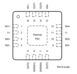
    Understood, I would use the OPA4990SIRTER, which comes in a small 3mm x 3mm package. 
    The circuitry would be as follows, 

    The op amp is powered in dual supply (±15V). 
    Ch1 and (Ch2 if you would like but not necessary) would be for the voltage output.
    Ch3 and Ch4 would be for the current output. 

    For the voltage output, I recommend the non-inverting configuration. Due to the stability concerns with the large capacitive load of the long cable, I recommend implementing a RISO + Dual Feedback solution (this improves stability while not sacrificing DC accuracy).  Listed below are my references: 
    Non inverting cookbook circuit 
    Riso + Dual feedback example 

    The second op amp (CH2) may be used in a buffer solely for toggling the SHDN pin but I do not think it is required as the CH1 could simply be used. 

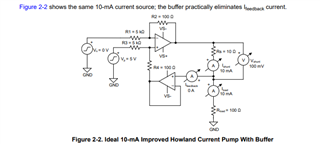
    For the current output, it can be achieved using the integrated solution of the XTR111 or it can be accomplished with an howland current pump solution.
    If you would like to proceed with the XTR111 solution please open a new thread with this part number so it may be answered by the 4-20mA signal conditioners experts.
    If you would like to use an pp amp, I recommend using channels 3 and 4 in the following configuration. Here is the reference for the howland current pump: 

    Analysis of Improved Howland Current Pump Configurations

    Again for stability concerns, implement the riso+dual-feedback for high DC accuracy. 

    I recommend then to use pins 6 & 7 to select the shutdown for each selection: 

    If the customer wants to use XTR111 for the current, then just do the first half of my answer with 1 OPA990S, since the second one (just for SHDN is redundant). 

    All the best,
    Carolina 

  • Hello Team,
    I have selected an opamp (MPN - OPA202IDBVR) from the TI store.
    The OPA202IDBVR is able to drive high capacitive load (up to 25nF) and can be used to drive up to 100nF if using Riso.
    Can I use this opamp to drive the 0 -10V analog output?

    If I am using this Opamp, I hope I don't need to design the dual feedback approach.
    Could you please comment on this

  • Hi Shibin,

    I would do it this way:

    shibin_opa202.TSC

    shibin_opa202_1.TSC

    I explain it later.

    Kai

  • Hi Shibin,

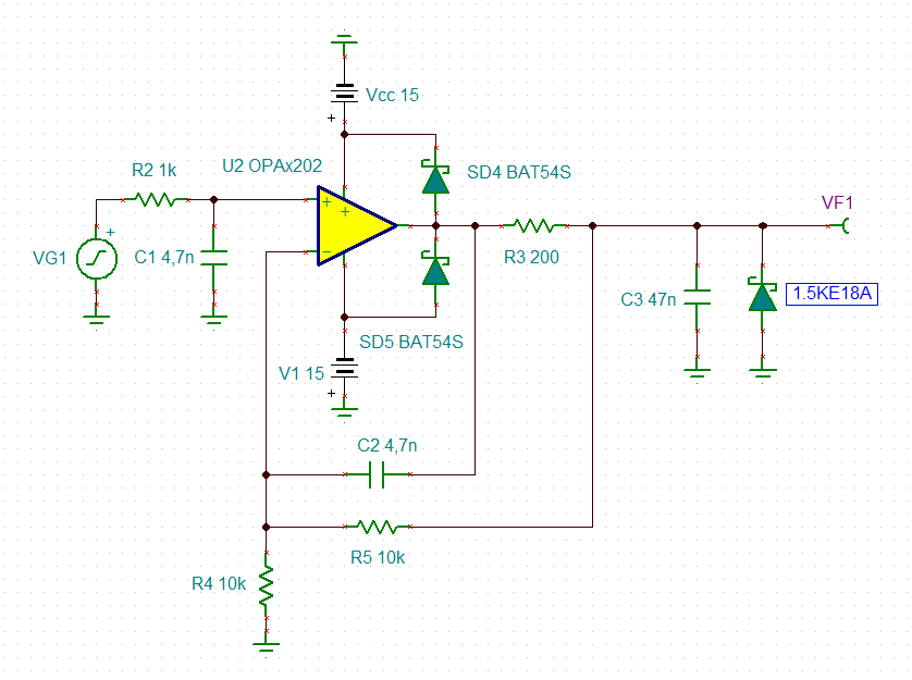
    It's essential for an industrial 0...10V driver to have a robust protection circuit against ESD, Surge, Burst and EMI at the output. So, mounting an uni-directional TVS from the output to signal ground and diode clamps from the output to the supply rails is mandatory, at least in my eyes. So, if I had to take the OPA202, I would eventually use this circuit:

    Not shown are the obligatory 100nF supply voltage decoupling caps from each supply voltage pin to signal ground! When heavy capacitive loads, like longer cables or similar, have to be driven, the decoupling capacitances can be increased to 470n...1µ or so.

    The 1.5KE18A is a very good choice when supplying the OPAmp with +/-15V. The reverse stand-off voltage of 1.5KE18A is 15.3V and the reverse breakdown voltage is about 18V, which means that even with the maximum output voltage of OPA202 the TVS cannot become conductive and that, at the same time, the supply voltage of OPA202 is clamped to a voltage below the absolute maximum rating of +/-20V during mild Surges. If heavy Surges can reach the output, you should connect additional 1.5KE18A from each supply voltage pin of OPA202 to signal ground, though.

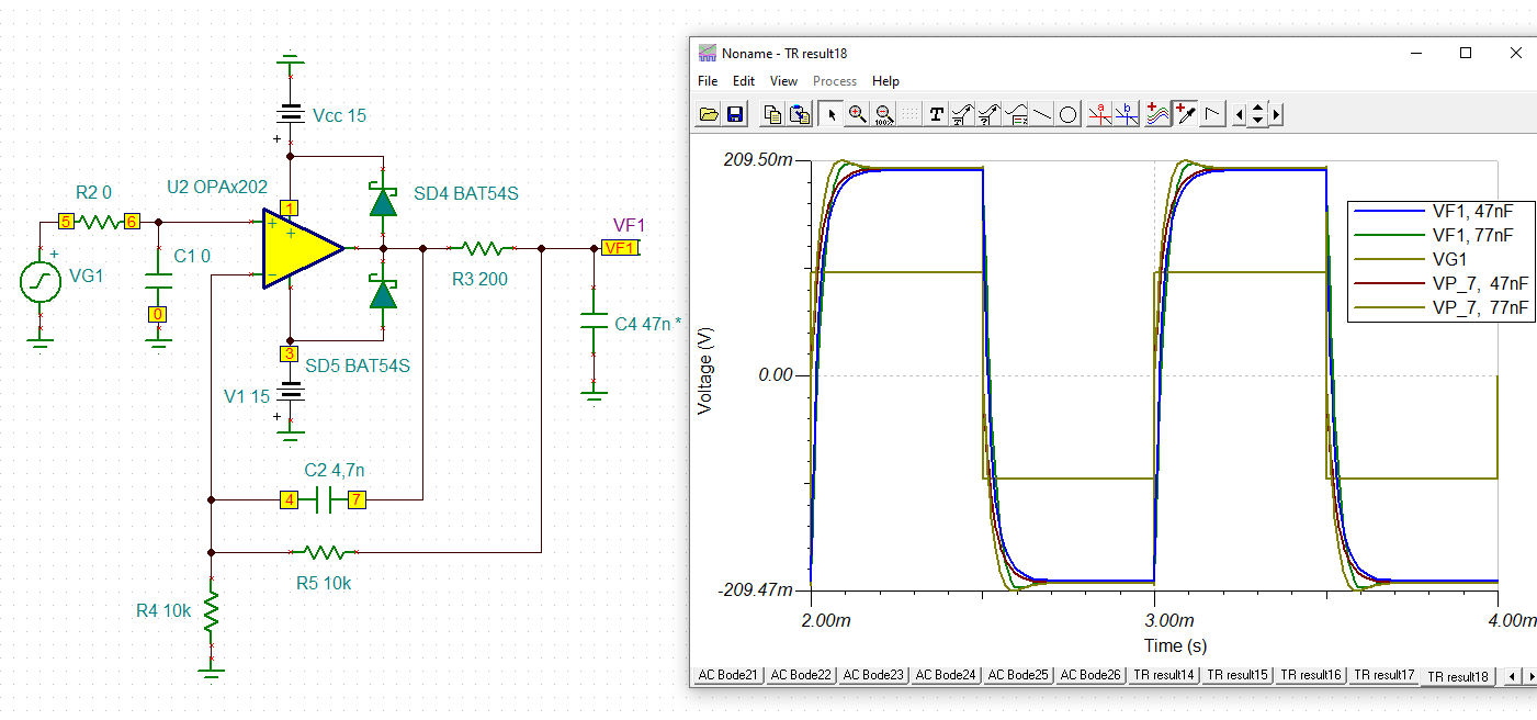
    SD4 and SD5 are Schottky diode clamps to the supply rails. To limit the current through these diodes, the current limiting resistor R3 is necessary. R3 also serves as isolation resistor in the dual feedback method. You can see, that because of the need of current limiting, it makes no sense to run this circuit without R3 or by other words to dismiss the dual feedback method.

    R3 is very helpful, if a Surge is reaching the output during a power-down of OPAmp. This is especially true when the above disussed additional 1.5KE18A TVS are mounted from the supply voltage pins of OPAmp to signal ground. Then, a big portion of Surge current would otherwise flow through SD4 and SD5 and eventually damage them.

    And R3 also plays a third, important role by helping to decrease the heat dissipation of OPAmp during a short-circuit event at the output of OPAmp. In critical cases R3 may even be increased so much that the short circuit current will be limited down to only a few mA. This can especially be helpful in battery powered applications when the current consumption is critical. So, you can see that it makes no sense at all to dismiss the dual feedback method and to not profit from the presence of isolation resistor R3. 

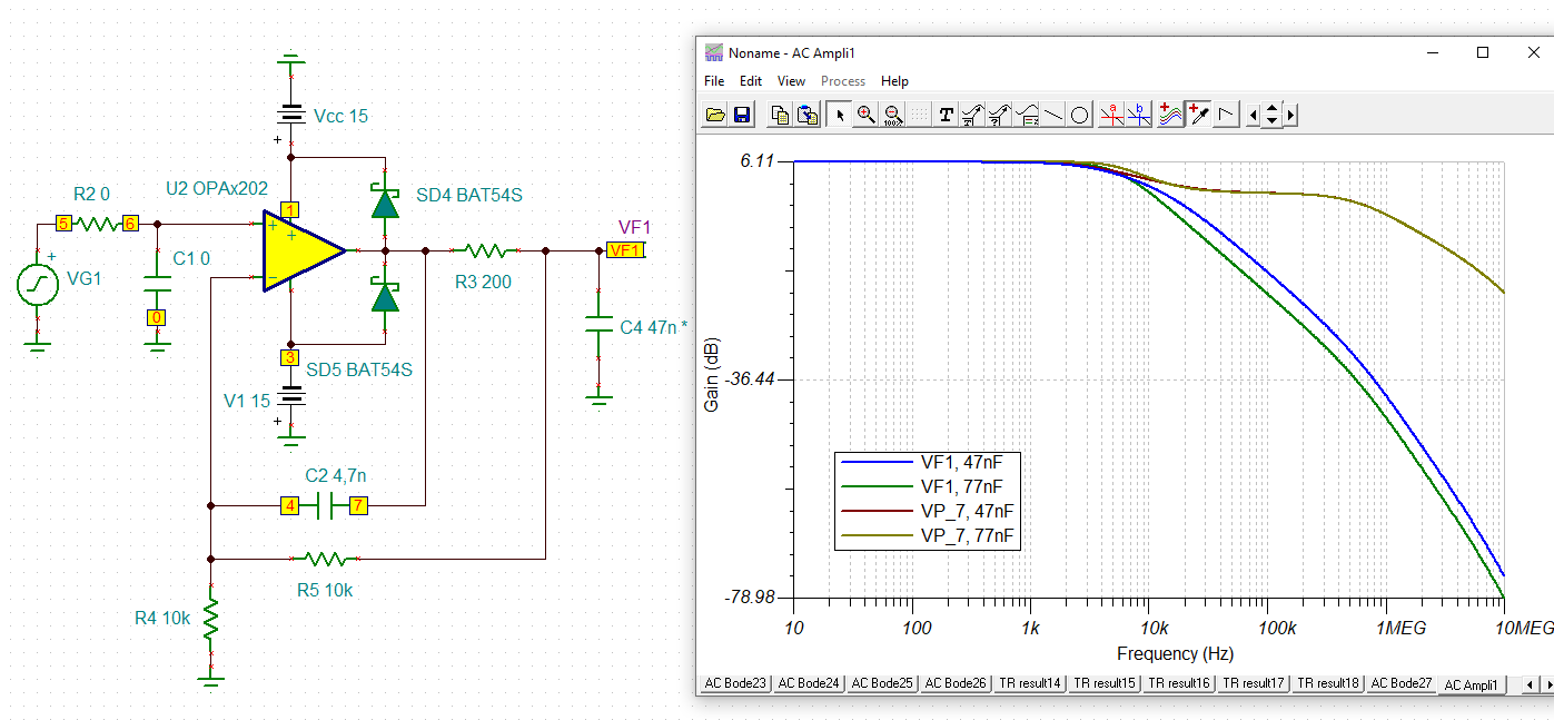
    Because the dual feedback method in many cases is only stable for a rather limited range of load capacitance, C3 should be chosen carefully then: C3 should dominate over the added junction capacitance of TVS, which is about 5nF for the 1.5KE18A, and the cable capacitance, which is about 100pF per meter. A 100m long cable adds about 10nF load capacitance. On the other hand, C3 should no be chosen too high, because the higher the load capacitance the more C3 looks like a short circuit for the higher signal frequencies. This can considerably limit the bandwidth of circuit.

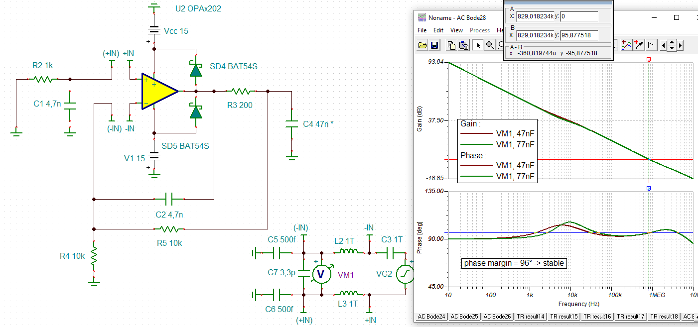
    The TINA-TI simulations in may earlier thread show the step response, the frequency response and the phase stability analysis for load capacitances ranging from 47nF to 77nF. If you want to make the circuit immune against higher capacitive loads, you may need to increase C2 accordingly to prevent a degradation of step response and frequency response.

    Kai