Hi:
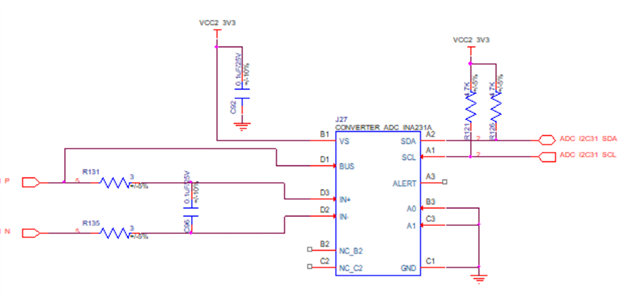
We used INA231a to test the current,At present, several INA231a ADC chips suddenly break down during use. The main problems are as follows:
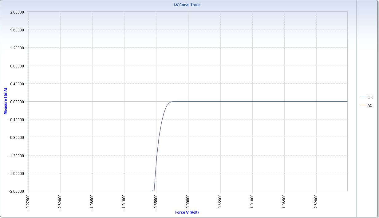
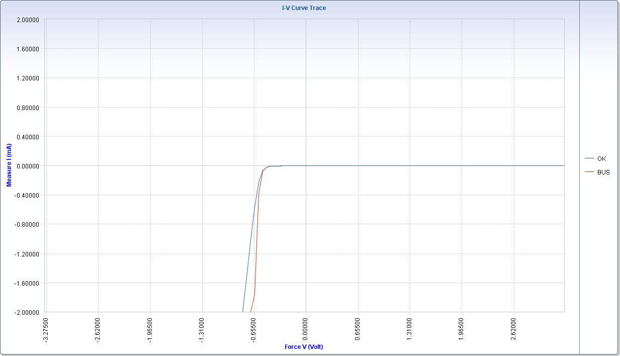
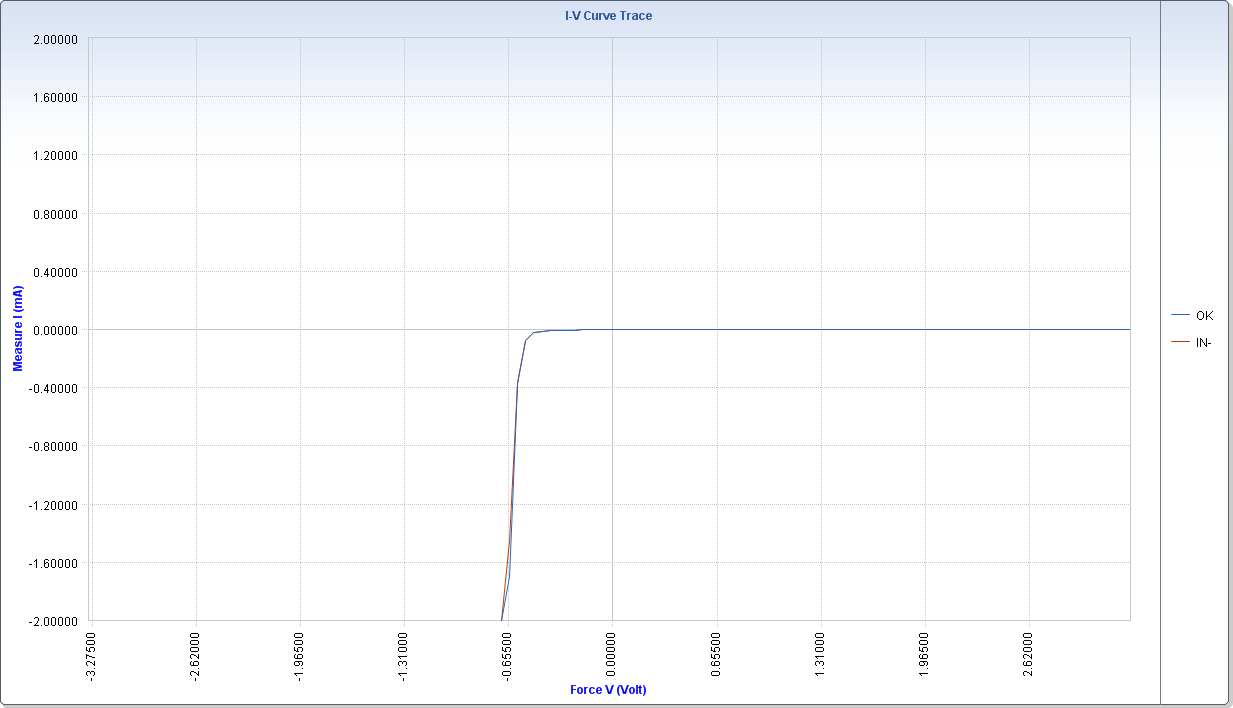
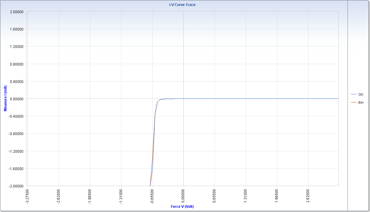
1. Vbus returned correct value at the beginning of ADC chip test, and 81.9V appeared in subsequent Vbus test (the actual voltage range of the device under test did not exceed 0-28v specified by ADC).
2. The phenomenon of 81.9V in Vbus test can be divided into two cases: 1) After the Vbus test of some ADC chips is 81.9V, the phenomenon of Vbus 81.9V will continue to appear in subsequent tests . 2) When the Vbus test of some ADC chips shows 81.9V, if the test scenario will be changed, and the Vbus test will become normal, that is, the test results are in line with expectations,but so far it has only happened once.
3. If 81.9V occurs continuously in the Vbus test, the return result of the Vshunt test is also incorrect .At present, we are unable to locate the problem based on the above phenomenon. I would like to consult with you to see if you can give corresponding solutions or suggestions to the above problems,Thanks.