This thread has been locked.

If you have a related question, please click the "Ask a related question" button in the top right corner. The newly created question will be automatically linked to this question.

OPA2227: Offset calculation

Part Number: OPA2227

Team,

my customer is comparing OPA2227U to OPA2227UA. Can you explain how to properly calculate the offset of the devices over temperature?

  • Add the temperature-dependent offset to the offset at 25°C ?

  • Add the temperature-dependent offset to the offset already given in the temperature range [-40;+85]?

How should the offset voltage in the range [-40;+85°C] be interpreted? 

  • Is the offset derivation already taken into account?
  • Is the max offset @85°C 100µV or 0.6µV*(85-25)+100µV?

Thanks

  • Hi Franziskus,

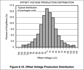
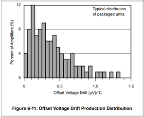
    Offset over temperature can be calculated using the offset at 25°C and the offset drift (dVos/dT). Both of these specifications have a typical and max value based on the gaussian distribution over process.

    For example, to calculate the typical device's Vos at 65° for the U package, you may use the following formula: VosTyp85 = 5 + 0.1*(85-25) = 11µV

    Of course, both the Vos and Vos drift specifications are +/- and therefore the polarity of the offset can be either negative or positive.

    Note that the Vos drift spec in the table is a linear approximation of the total drift across temperature, and the calculation above should be thought of as an estimate or typical value, rather than an exact value. The exact Vos over temperature is affected by process variation and the non-linear dVos/dT curve.

    This is why the datasheet specifies the max offset over the temperature range. This specification considers the process distribution of voltage offset at 25°C, the process distribution of offset drift, and the non-linearities of the drift over temperature. This max specification is the worst case over the temperature range, whereas the calculation above is an estimate for operation within that temperature range.

    Thanks,

    Zach

  • One quick correction: the example calculation above is for the typical device's Vos at 85°C, not 65.

    Is the max offset @85°C 100µV or 0.6µV*(85-25)+100µV?

    The max offset for OPA2227U @85°C is 100µV as given from the spec table.

    Thanks,

    Zach

  • Hi Franziskus,

    there's a nice appnote on this topic:

    sloa059b.pdf

    See section 5.3.

    Kai

  • In the case of bipolar transistor input stage with large offset (e.g. |Vos|>1mV), Vos and offset dirft are correlated with one another: drift=~Vos(25)/298C

    Thus:  max_Vos[@65C] = max_Vos(25C) + delta_T * max_Drift = +/-75uV+/-(65C-25C)/*0.6uV/C = +/-99uV  (linear addition)

    In the case of CMOS or JFET transistor input stage offset and offset drift are NOT correlated and thus offset and drift must be added as vector quantities:

    max_Vos[@65C] = [(max_Vos(25C)^2 + (delta_T * max_Drift)^2]^0.5 = +/-[(75^2) + (24^2)]^0.5 = +/-79uV

    Since OPA2227 is bipolar input op amp with very low initial offset of +/-75uV, the max value of Vos at 65C will be somewhere between +/-79uV and +/-99uV.

  • Thank you all for you helpful replies!

  • Hi Franziskus,

    Happy to help. I will go ahead and close this thread for now.

    Feel free to reply again if you have any more questions.

    Thanks,

    Zach