Hello,
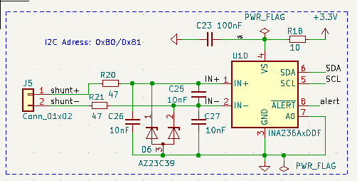
I was using the DSBGA Version of the chip for high side (+12V) current measurement. Now I redesigned the board to use the DDF package.
With this new version I can successfully communicate (I2C) and measure currents only when on low side (GND) related shunt. As soon as I try to go with the common voltage > 0.7V the device starts to clamp and I cannot use it for high side measurements in the +12V region.
I verified the board and only the INA236 makes this trouble when mounted on the board. When injecting voltages > 0.7V on either IN+ or IN- the pin starts to draw current. I have verified this behaviour and all 3 devices for testing.
Have you veered high side > 0.7V operation for the DDF packaged devices?
Best regards
Kai

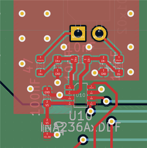
note: D6 is NOT in the actual layout and therefore not mounted.

note: inner layer In2 (GND plane) not shown. Inner layer In1 top half GND and lower half +3.3V.


