This thread has been locked.

If you have a related question, please click the "Ask a related question" button in the top right corner. The newly created question will be automatically linked to this question.

OPA828: Package influence on input bias current

Part Number: OPA828
Other Parts Discussed in Thread: LF356,

Asking on behalf of customer.

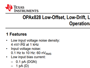
According to first page of datasheet, input bias is 10x different DGN package vs. D package.  

What is driving this discrepancy?

Contact me internally if further details needed. Thanks!

-Steve

  • Antenna,

    I'm checking with the design team on this.  The package material and molding compound will have some impact, but at room temperature I would expect the numbers to be closely.  Also, note that I see a 5x difference at room temperature for typical (0.2pA vs 1.0pA), and a much smaller discrepancy for maximum (at room temperature only).  Over temperature, the to devices share the same specification.  I just want to clarify that we are looking at the same information.  

    Best regards,

    Art

  • See datasheet page 1- this is what customer noticed, see input bias near bottom:

  • Antenna,

    The front page is really a typographical error and you should rely upon the specification table.  I got some feedback from the device designer regarding the discrepancy between the input current for the two packages:

    The discrepancy is mainly due to test improvements that were made between the release of the D and DGN package.  From the perspective of the bias current the two packages should be equivalent.  So, the D package leakage should generally be lower than what is currently specified.  Nevertheless, it is really best to design according to what is in the data sheet table so I would use the values in the table when doing any error calculations.

    Best regards, Art

  • Hi,

    maybe I'm wrong but I think the package style has an impact on the input offset voltage and input bias current of OPAmp and other specifications which rely on a high symmetry of internal circuitry, like the common mode rejection ratio for instance.

    Let me tell you a little story: Many years ago when low input offset voltage FET-OPAmps were rare and expensive I took the LF356 in DIL8 package and hand-selected a handful of OPAmps for lowest input offset voltage (<0.1mV). To my surprise, after soldering the OPAmps directly into the printed circuit board afterwards, the input offset voltages were no longer <0.1mV but varried up to 2mV. It turned out that during the hand-selecting I pushed the LF356 into my test-DIL-socket and mechanically stressed the package. By this pushing the die seemed to be bended and twisted slightly what caused a shift of input offset voltage. The mechanical stress had an impact on the symmetry of circuitry on the die and the two input FETs no longer behaved evenly.

    Mechcanical stress on a semiconductor can also result in higher leakage currents because of an increase of defects in the crystal lattice which may increase the number of charge carriers in the conduction band.

    So, since the "DGN" package seems to be more torsion-resistant and more robust against bending compared to the "D" package, the OPA828 in the "DGN" package may show a narrower statistical scattering of input offset voltage, input bias current and common mode rejection data. Not much, of course, because the mechanical stress during the chip testing is rather moderate.

    Only an idea Relaxed

    Kai

  • Kai,

    I completely agree on offset, offset drift, and on many other parameters.  However, for this device I spoke with the characterization and design engineers.  The two package variants were released at different times and improvements were made in tester capability.  The design and test team believe that the room temperature Ib is relatively independent of package.

    best  regards, Art

  • Thanks Relaxed

  • Just to add my 2 cents, soldering the part causes a thermal shock twisting/bending the part inside the package due to different expansion ratio between die, lead frame and package itself - this effects mostly Vos and drift.  These are temporary shifts that for most parts over time go away on their own BUT at room temperature may take few day to a week to fully recover.  In order to accelerate this process, it is advisable to burn-in (unbiased) assembled PCB in high temperature oven in order to accelerate the stress-relief process. Few hours at 100C or 30 min at 125C typically returns the offset and drift back to their pre-soldering conditions.  A note of caution, please make sure that all the PCB components are rated for the temperature you plan on using for burn-in.