Part Number: BUF802
Hi team,
One of our customer's issues, I'm forwarding it below, could you please provide some troubleshooting suggestions?
The design parameters are designed in accordance with section 11.2 of BUF802DATASHEET, and the input port is high resistance configuration
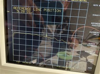
The parameters of the test input port S21 are shown in Figure 1 below, and the test point is the high-frequency part after C26

Figure 1 Curve of S21 after signal port to C26
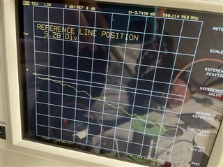
After the test output port passes a 50 ohm resistance, the S21 curve of the high frequency part of the signal is shown as the figure below:

Figure 2 Curve of output port S21
Why is the test output -3dB bandwidth gap so big?
The purpose is to adjust the high-impedance input chain with a bandwidth of -3dB and 1Ghz. The schematic design is shown in Figure 3 below

FIG. 3 Schematic diagram of buf802 design
Best Regards,
Amy Luo

