This thread has been locked.

If you have a related question, please click the "Ask a related question" button in the top right corner. The newly created question will be automatically linked to this question.

LPV812: Transimpedance Amplifier

Part Number: LPV812

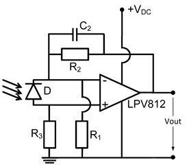
Is anybody aware of the transimpedance amplifier circuit shown below? I found it in an old textbook but unfortunately without further explanations. R1 and R2 seem to form a non-inverting amp, but I am not sure about the function of R3. And the non-inverting circuit is normally not used with transimpedance amplifiers. Has anybody seem this circuit elsewhere?

  • Hi Frank,

    A similar TIA circuit is shown on "Photodiode Amplifiers" by Jerald Graeme on p.154, where the photodiode is connected across the inputs of the amplifier.

    This circuit is useful for high-gain photodiode amplifiers.  In the standard transimpedance amplifier (TIA), making the feedback resistance large produces high gain, but using very high resistances often introduces performance limitations, sensitivities to stray capacitances, and a reduction of bandwidth.

    This circuit adds voltage gain (1+R2/R1) in a single stage TIA topology while allowing the use a smaller RF resistor.  Essentially, in this transimpedance circuit, the current of the photodiode will flow through RF as shown below.  The effective transimpedance gain is given by:

    RT= RF*(1+R2/R1)

     The resistances of R2 and R1 of the feedback network are kept relatively low compared to RF.   Connecting the photodiode across the amplifier's input terminals bootstraps the diode, where the voltage across the photodiode is kept near ~0V, where the diode bias voltage does not see the voltage swing RF*Idiode, providing a linear response.

    Thank you and Kind Regards,

    Luis

  • Hi Frank,

    a disadvantage of this circuit that it can generate considerably more noise:

    frank_diff_tia_2.TSC

    By the way, exactly spoken the transimpedance is

    (1 + R2 / R1) x RF + R2

    But the last summand "R2" can be neglected in most cases.

    Kai

  • HI Kai,

    The exact equation includes the R2 summand term.  In many cases the last term R2 could be neglected since resistors R1 and R2 are kept considerably smaller than RF.  In some very high gain transimpedance cases, this approach allows for the high gain without very large resistors, reducing some of the sensitivities to stray capacitances, with the trade-off in noise.  Another method for high gain is the transimpedance amplifier with the T-network, which also allows the use of smaller gain resistors, but also exhibits higher noise compared to using a single resistor in the feedback:

    https://e2e.ti.com/support/amplifiers-group/amplifiers/f/amplifiers-forum/1207724/opa657-tia-with-a-feedback-t-network?tisearch=e2e-sitesearch&keymatch=t-network%2520transimpedance#

    Most practical applications that require a high transimpedance gain while meeting bandwidth requirements, and relative low noise, often add a second amplifier stage for gain, in a multistage design.  The transimpedance gain of the first stage is set while meeting the bandwidth requirement, and the noise performance is managed while adding filtering on the second gain amplifier stage.

    Regards,

    Luis 

  • Thank you, Luis! That is exactly what I was looking for.

    Regards, Frank

  • Thank you, Kay. This is quite helpful for your prototype circuit!

    Regards, Frank