This thread has been locked.

If you have a related question, please click the "Ask a related question" button in the top right corner. The newly created question will be automatically linked to this question.

OPA455: Quiescent current.

Part Number: OPA455
Other Parts Discussed in Thread: OPA593, LM2876

Hi TI team,

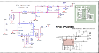
   I am using third party (Boost/SEPIC/Inverting Converter) converting +ve 60V to -ve 60V which provide output current 10mA. With this supply I am connecting OPA455 +Vs = 60V and -Vs = -60V. While connecting my OPA455 output voltage of the 3rd party converter drops to -ve 5V. In OPA455 datasheet I found Iq is 3.7mA max. kindly help me to solve this issue.

Regards

Saravanakumar D 

  • Hello Saravanakumar, 

    Can you provide a schematic? I have a few questions to start the discussion. 

    1) Do you have decoupling capacitors on the supply lines close to the supply pins of the OPA455 with a low impedance return to ground?

    2) At what voltage level are the pins ED and ED Com being set to in this condition?

    3) What potential is the power pad soldered to?

    Best Regards, 

    Chris Featherstone

  • Hi Chris,

    Thanks for your reply,

    Schematics for your reference. 

    1. Do you have decoupling capacitors on the supply lines close to the supply pins of the OPA455 with a low impedance return to ground?

    Ans : Yes decoupling is connected 

    2. At what voltage level are the pins ED and ED Com being set to in this condition?

    Ans : Pins Not connected 

    3. What potential is the power pad soldered to?

    Ans : Power pad connected to negative supply pins

    Regards

    Saravanakumar D

  • Hello Saravanakumar, 

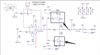
    Have you already isolated the issue to the OPA455, meaning that the output is disconnected from the transistor network as shown below? I just wonder if it is possible that excess current is being pulled out of the amplifier's output during startup. In the meantime I will review your schematic and see if I can identify some suggestions. If you are able to provide any additional information regarding the third party (Boost/SEPIC/Inverting Converter), this could also be helpful for debugging. 

    Best Regards, 

    Chris Featherstone

  • Thanks!!!

    We Isolated Transistor circuit and tried. Still same problem exist. I can share the screenshot of the 3rd party converter schematics.


    Kindly clarify my doubt : That transistor circuit is to Boost the current. Will it work with circuit ?

    Regards

    Saravanakumar D 

  • Hey Chris,  

    We solved the issue now we are getting required proper output from OPA455 with E/D and E/D Com floating. 

    Changes Done : We reduced the input voltage 60V to 15V on the 3rd party inverter since it is a BOOST topology it worked properly.  

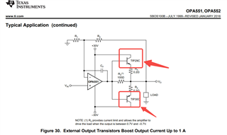
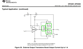
    1. Now the issue is to boost the output current of my op amp. I have used the same reference circuit suggested by TI, in that I have changed the part number for NPN and PNP BJT's. kindly check and tell us weather this circuit will work to deliver the current up-to 500mA.  Schematics given below


    Ans : ?

    2. Since my + and - ve source current is verry less I can't connect the source at collector pin's of NPN and PNP transistor's. Shall I connect +15V and -ve 15V instead of + or - 60V as show in below schematics. 


    Ans: ?

    3. How to calculate R4 and R3 resistor and explain how ?

    Ans : ?

    Regards

    Saravanakumar D 

  • Hi Saravanakumar.

    1. Now the issue is to boost the output current of my op amp. I have used the same reference circuit suggested by TI, in that I have changed the part number for NPN and PNP BJT's. kindly check and tell us weather this circuit will work to deliver the current up-to 500mA.  Schematics given below

    The circuit should be able to source up to 0.5A output swing, but the BJTs heat dissipation depend on the input supply voltage and output voltage swings, where (Vs - Vout)*Ic = 0.5*(Vs - Vout) will be the heat dissipation across the current booster driver. I need additional information how you are planning to drive the output. If Vs - Vout is large, then the BJT will dissipate higher heat, may or may be able to handle to energy dissipation without heat sink. 

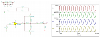
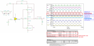
    I have imported the complementary BJTs that you are suing, but the PSpice models have issues, see the simulation. See the current source of 2.82A at Vin = 0, where something in the model is gone wrong or partially shorted. Attached is the bad model FYI.  Please provide me a working model, and I am able to simulate the condition. 

    BJT Driver Issues 05082023.TSC

    2. Since my + and - ve source current is verry less I can't connect the source at collector pin's of NPN and PNP transistor's. Shall I connect +15V and -ve 15V instead of + or - 60V as show in below schematics. 

    If the application's output is within +/-15Vpk, then you should lower the ±supply voltage. The heat dissipation across the BJT current booster will be higher, if delta voltage (Vs - Vou) is larger. Also, the setup may require the heatsink on the BJT, depending on the heat dissipation. So lower the supply voltage, will reduce the heat dissipation of complementary BJT driver, and increase the driving efficiency. 

    3. How to calculate R4 and R3 resistor and explain how ?

    R4 or 0.2Ω are the degenerative resistor, it will reduce the BJT's current gain, and increase BJT's linearity, perhaps decreasing the distortion effects. R3 or 100Ω should provide certain voltage and current when the output voltage swing below Vbe (~0.65V) of either transistors. There will be some distortion on the current booster circuit, but you may be able to minimized the distortion when R3 is configured properly. 

    You should check out in the simulation and see the effect of the Ioa's output current for a given load. Also, the schematic has capacitive coupling with 0.1uF capacitor. The capacitive coupling cap has impedance of 1/sC or 1/(2*pi*f*C). I do not know what you are driving, the capacitor may reduce the output current at the load. I need the driving requirements in order to optimize the circuit.    

    OPA455 20Vpp Diode 03032023.TSC

    Once you finalize the current booster circuit, we can check for the stability, where R4 (0.2ohm of your schematic) may play a role somewhat . OPA455's Ioa may swing up to 40mA or so (<45mApp) , and will provide very coarse current limiting capability in the circuit. However, the circuit current boost stage does not have current limiting, and it is possible that the BJT may get damaged or get very hot, if the output is shorted to ground or supply rails etc.. 

    If you want to check out the stability, linearity etc., you would need to provide us with a working PSpice model on the BJTs. Otherwise, I am unable to provide you with the information on the actual circuit.  If you have additional questions, please let us know. 

    Below is the transistors that I used for the simulation. 

    https://www.mouser.com/ProductDetail/Diodes-Incorporated/ZX5T853GTA?qs=wnTfsH77Xs4gLjmmzHX6GQ%3D%3D

    https://www.mouser.com/ProductDetail/Diodes-Incorporated/ZX5T953GTA?qs=MQZxQ7B7MZJRoUtuaHvteg%3D%3D

    Best,

    Raymond 

  • Hi, 

    Thanks,

    Our BJT Supply Voltage is same as the OPA455 +Vs +60 and -Vs -60. Vout = 108Vpp,freq = 2.4kHz and load current is 120mA. We are driving the LVDT which has Primary DC resistance of Res = 120ohm.

    1. In this case Power dissipation of the BJT Pd = 0.12A(120V-108V) is that right ?

    Ans?

    2. We are driving LVDT from the output of BJT. To limit the current shall I change the R84 value from the diagram shown below.  I want to limit the current  to 150mA  for the initial testing.

    Ans?

    Regards

    Saravanakumar D


  • Hi Saravanakuma,

    1. In this case Power dissipation of the BJT Pd = 0.12A(120V-108V) is that right ?

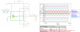
    You presented one of peak power of the BJT transistor. Since this is AC output, you must integrate the AC power under the curve, which is the average power dissipation in upper and power BJTs, as shown below. 

    If I assumed the BJT pairs that driving the load, the upper BJT dissipates approx. 0.6W, and lower BJT dissipates approx. 0.65W. 

    As the example, the junction temperature of the upper BJT will rise approx. Tamb + 6.3C, if you follow the manufacture PCB layout configuration, and the part will not overheat up to Tamb of 85C, perhaps higher.  

    We have other ways to simulate the heat dissipation, but this way may be easier to understand, if you check out the post-processing calculation in the attached simulation file. 

    OPA455 108Vpp Power Simulation 05092023.TSC

    2. We are driving LVDT from the output of BJT. To limit the current shall I change the R84 value from the diagram shown below.  I want to limit the current  to 150mA  for the initial testing.

    To have current limit in the driving configuration, you have to include a current limit circuit for the complementary driver. If the PCB is already made, it is not so easy to implement. R84 does not limit the output current from BJT drivers, and it does not have the control to limit the current down to +/-150mA at output stage. I mentioned previously, it may have a coarse current limiting feature since OPA455 is going to clamp the op amp's output voltage when its max. output current is reached approx. +/-40mA.

    Since this is LVDT application, the circuit is driving a transformer. I recalled that Kai and I recommended a differential output drive for the application. Now I see why you are using capacitive coupling at the output stage. 

    With the differential output drive, the output stage may be coupled to transformer directly or via capacitive coupling. If the differential transformer has a fixed DC biasing voltage at its primary side, there is no DC current flow within the primary coil and hence the transformer will not be saturated. In you case, the transformer is capacitive coupled and one side is connected to ground. 

    To have a current limit at approx. ±150mA in the complementary drive, you would need this type of current limit design. Or you can current limit your power supply rails for the ±60Vdc. 


    Please let us know if you have additional questions. 

    Best,

    Raymond


  • Hi Saravanakuma,

    Here is an example that you could drive the LVDT application, which is using our OPA593.  You may configure different configuration to drive the transformer, and OPA593 will have fairly accurate current limiting features. In addition, you will need single 60Vdc supply to drive the application, and save some PCB real-estate. 

    Please let me know if you are interested the option (I did not optimize the schematic, presented it as a quick example). You may also use some of our audio amplifier driver to accomplish the similar drive with some pros and cos considerations.  

    OPA593 2p4kHz Transformer Driver 05092023.TSC

    Best,

    Raymond

  • Thanks for your support,

    Now BJT combination we are getting required output. 

    1. If we don't want current limiting circuit for my application, with the existing BJT circuit is it capable to drive LVDT?

    Ans?

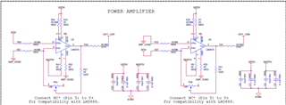
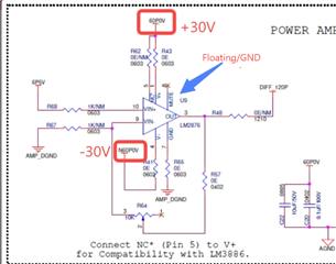
    Yes we have added differential output drive circuit as per your recommendation by using LM2876 audio amplifier but we did not add current limiting circuit as shown above picture.  Vin = 6.5Vpp


    2. To drive LVDT this above circuit is enough without current limiting circuit ?

    Ans ?

    Regards

    Saravanakumar D 

  • Hi Saravanakumar,

    1. If we don't want current limiting circuit for my application, with the existing BJT circuit is it capable to drive LVDT?

    It should be acceptable. LM2876 will have limited protection as prescribed in the description. It is not ±150mA current protection, but it will protect against the destruction of the power amplifiers, if faults are occurred for some reasons. I think that the application transformer may be ok since it has impedance approx. 450Ω or range or DC winding resistance is over 100Ω+ or so. 

    2. To drive LVDT this above circuit is enough without current limiting circuit ?

    I think that it will be ok, the LM2876 is capable to protect itself by design, please check with the transformer's power rating also. 

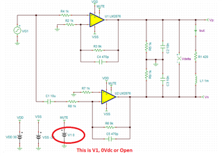
    The application schematic should work below. Since you are driving inverting and noninverting node at input, please make sure that the output, circled in orange has the identical DC offset voltage (no significant DC offset voltage or drift that will result the saturation of the transformer). If it is difficult to achieve, then you may connect the output via capacitive coupling to the transformer (remove the DC components). If you are treating the output as a balanced differential driving signals (volt-second balanced), then BH curve of the transformer (magnetic core) should reset itself and should not result in a saturation over time.   

    My example above is using the fixed Vcm to drive both op amps. so the output DC operating point should be very close or near identical, which it may minimize the magnetic saturation. But the op amps' input is driving into inverting nodes, which it has lower input impedance than non-inverting input nodes. These are pros and cons that you may consider.  

    If you have additional questions, please let me know. 

    Best,

    Raymond

  • Thanks for you support,

    We are planning to use LM2876 to drive LVDT.

    1. We are not able to get output from LM2876 Op-amp. We found some mistakes in the existing circuit and we corrected it by adding external wire to it. The changes are given below 

      i. Supply voltage reduced to + or - 30V as per the data sheet.

     ii. Mute pin resistor Rm connected 10K. 

     iii. Vin - 6.5Vpp

    Note : After those changes we are not able to get the output

    Ans?

    Kindly suggest what will be the issue and help us to resolve this.

    2. Why mute pin resistor Rm is required in LM2876 if it left open what will happen.

    Ans ?

    Regards

    Saravanakumar D 

  • Hi Saravanakumar,

    After those changes we are not able to get the output

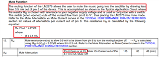
    Normally, there is a switch for the Mute function. When pin8 is left open or 0V, Mute = OFF. When Pin8's current > 0.5mA, Mute=ON. so you should remove 10kohm or place a switch or GPIO controlled switch circuit on that pin. 

    2. Why mute pin resistor Rm is required in LM2876 if it left open what will happen.

    You should leave pin8 open, then the output voltage will be engaged. If you want to control the On/Off of the transformer in your application, then you may require to control the current flow out of the pin. 

    If you have additional questions, please let us know. 

    Best,

    Raymond

  • Hi Raymond

    FYI initial design Mute pin 8 is left open, even though we didn't get the output.

    Any other suggestion to enable the output. ?

    Ans?

    Is it mandatory to connect the load ?

    Ans ?

  • Hi Saravanakumar,

    Any other suggestion to enable the output. ?

    It should work, unless your output is reached saturation or similar, and the output is disabled by fault protection circuit. 

    Vs: ±30Vdc with the previous schematic

    Input: 2.7Vpp. 2.4kHz

    Output: ~102Vpp

    LM2876 Transformer Driver 05102023.TSC

    Best,

    Raymond

  • Hi raymond

    Mute Pin you connected 10V right ? Shall I try connecting the same ?

    Regards

    SK

  • Hi SK, 

    This is V1 on MUTE, 0Vdc or Open. I do not know what is your issue. Please check your connection and your load, make sure the transformer is not saturated. Use a know resistor, say 450Ohm to test the circuit. the Load or transformer's primary is floating under the configuration. 

    If you have other questions, please let me know. 

    Best,

    Raymond

  • Raymond,

    Thanks!!!

    Sorry, That was my mistake I didn't look into it properly. Mute pin connected to 0V.

    The issue is I am not getting the output from LM2876. 

    Without connecting the load resistor or load LM2876 won't deliver the output?

  • Hi Raymond,

    I don't know what may be the issue I can't turn ON LM2876. I am not getting any output. 

    Supply Voltage (V+, V-):  + or - 30V

    Input voltage Vin: 6.5Vpp.

    Mute Pin: Connected to Ground or left floating.

    Note : We didn't connect any load on the output.

    Kindly help us to solve this issue.

  • Hi SK, 

    I have to ask the part's purchasing question. Were these parts purchased from TI authorized distributors or TI E-store? There are many counterfeit parts, and I am unable to figure these out, if the parts are not authentic. Please let us know. 

    Also, please connect pin8 to -30Vdc via 10kΩ to 30kΩ resistor, this will draw >0.5mA current out of pin8, which it should turn Mute Off.  

    Best,

    Raymond

  • Hey Raymond,

      Its working as we expected THANKS for your support.

    OPA455 is heating too much. Any possibilities to reduce the heat?

    Regards

    Saravanakumar D 

  • Hi SK, 

    OPA455 is heating too much. Any possibilities to reduce the heat?

    I recalled that the design is using LM2876. Can you explain why OPA455 is over heating? I need the setup details. 

    I simulated it previously that OPA455 in the following configuration should dissipate approx. 0.6W. Do you mean that LM2876 is overheating too much?

    Best.

    Raymond

  • Hey Raymond,

    Yes you are right. But we are not using LM2876 circuit. Now we are using OPA455 circuit to use single ended output for one of our application. We cant reach 36Vrms required output voltage because of the overheating. Is there any other solution to reduce it. 

    FYI :- LM2876 also having overheating issue.

    Regards

    Saravanakumar D 
  • Hi SK, 

    Now we are using OPA455 circuit to use single ended output for one of our application.

    The following circuit will only overheating if the output voltage swing is low, which result in large voltage drop from (V+ - Vout) or (V- - Vout). Increase the resistor R81 from 100Ω to 500Ω or up to 1kΩ, this should reduce the heat dissipation in OPA455. 

    What is the actual load that you are using during the test? You should simulate these on your own, since I provide you with all the simulation files. 

    Also, how to you dissipate heat from PCB layout for OPA455 and LM2876. You have to use min. 2oz copper and increase large dissipated heat area on the PCB. Otherwise, you will have overheat issues in either configurations.

    Best,


    Raymond

  • Hey Raymond,

     Thanks for your suggestion, After mounting 500ohm the heating reduced to some limit but it is is oscillating low to high limit. I checked PCB fabrication info it was 2oz copper. Actual load is 120Ohm DC resistance LVDT. We are simulating using another 3rd party simulation tool. TINA we are not able to get those waveforms as you shown in the previous chat.

    Regards

    SK

  • Hi SK, 

    You have two similar driving circuits, and you need to tell me which one that you are working on, because the heat dissipation between two circuits are different.  

    Based on the information, my guess is that you are using OPA455. If the DUT is configured as simulated, it should not overheating. The reasons are that all the power dissipation is placed at the current booster. Unless there are typos in the wire or PCB connection, minimum load is placed on OPA455 driver. Could you send me the simulation file that you are working on? I need to see how the current booster is implemented in the actual testing conditions. 

    If you are using LTSpce, you can check the power dissipation in OPA455 readily. If you are using other simulation tool, you can use the similar method that I did in TINA and calculate the heat dissipation in OPA455s. 

    If I replace the load with 120Ohm, the current booster will dissipate over 2.5W of power, but OPA455 should not overheat based on the simulation. This is with 100Ohm. Is it possible that the OPA455 overheating is resulted from the poor heat dissipation on the PCB, where heat generation from the current booster is transferred to the OPA455? Please confirm.  

    Are you driving OPA455 to the transformer as shown above (Capacitive coupled)? What is the L, C parameters of the transformer. ESL = 120Ohm, I need to know L and C.  Or the transformer is being driven in a floating manner. 

    There is another possibility, which is related to power factor correction. You need to tell me L, C parameters of the transformer, and use the actual parameters in the simulation.  

    Best,

    Raymond

  • Hey Raymond,

    Is it possible to share your Mail ID. I will share more information of my project.

    Thanks 

  • Hi SK, 

    Please send me "friendship" request via E2E forum, which it has E2E private messaging. Once we have established the communication, we can communicate privately. 

    Best,

    Raymond

  • Hi SK, 

    I am going to close this inquiry, since we have established email communication.

    Best,

    Raymond