Hi Expert,
I do not understand how to understand figure 18. May I have your help to explain the relation for VCM.
Thank you.
Thank you.
This thread has been locked.
If you have a related question, please click the "Ask a related question" button in the top right corner. The newly created question will be automatically linked to this question.
Hi Expert,
I do not understand how to understand figure 18. May I have your help to explain the relation for VCM.
Thank you.
Thank you.
Hello,
It helps to use the Analog Engineers Calculator that can be found here:
https://www.ti.com/tool/ANALOG-ENGINEER-CALC
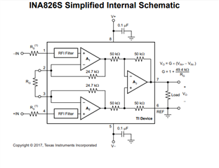
Due to the complexities of the 3 amp instrumentation amplifier it can be difficult to understand the min and max operating ranges of the input and output with various gain, and common mode and reference voltages. For this reason we often use Tina Ti and the engineering calculator together in order to determine the linear operating ranges. Below you can see the simplified schematic.
Referencing the product datasheet plot and entering in the tested PDS conditions for power supply, gain, Vref and Vcm we can recreate the plot in the product datasheet. The calculator provides the max and min input differential signals that can be applied to the INA826s in this configuration and still be in the linear operating region. 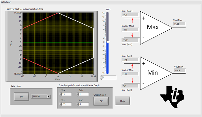
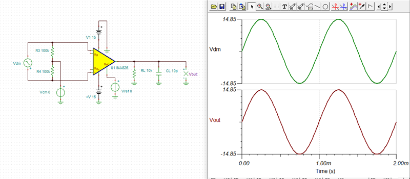
Using Tina and applying the 14.85 differential signal we can see that the output signal is 14.85. This matches the max output voltage that the calculator gives.
Alternatively we can apply the minimum input differential signal of -14.9 V the calculator found. You can see that the minimum output voltage is now -14.9 as predicted by the calculator.
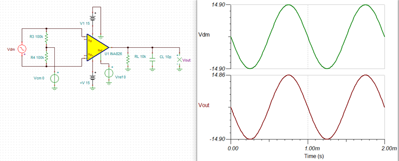
Applying an input differential signal greater/lesser than what the calculator shows will result in one or all of the internal amplifiers to enter the non-linear operating region and this in turn causes the INA to enter into a non-linear operating mode. The result will be signal clipping and distortion.
In the PDS plot you can see that if the input common mode voltage were increased to 8V, the min and max input and output voltages are now reduced.
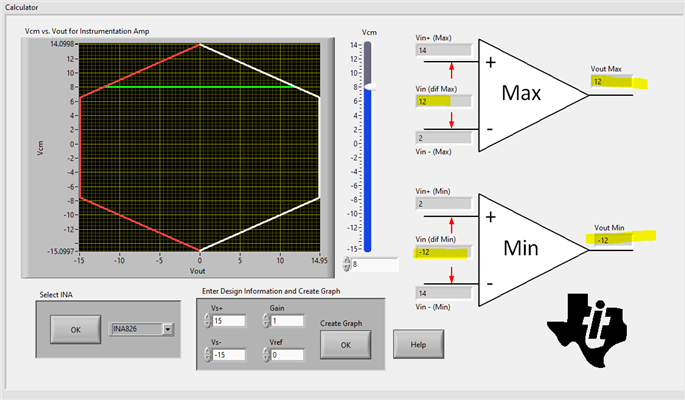
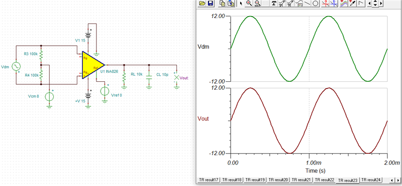
This is confirmed in simulation.
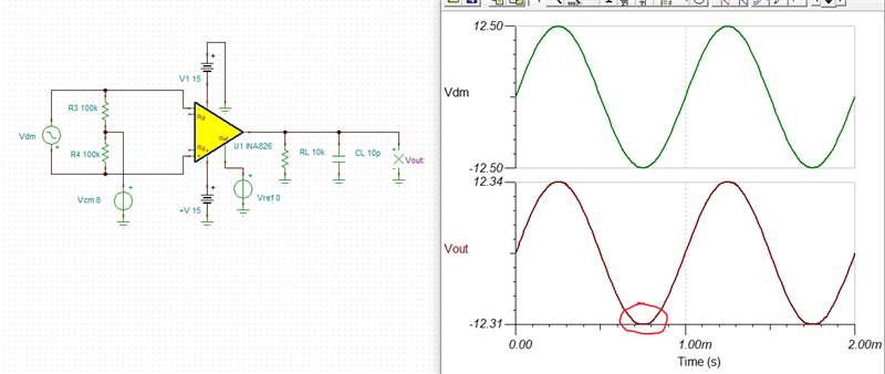
Using an input differential signal of 12.5V we can start to see subtle clipping occurring as I circled in red below.
I hope these tools and this explanation help clarify how to read the plots.
Best Regards,
Chris Featherstone