This thread has been locked.

If you have a related question, please click the "Ask a related question" button in the top right corner. The newly created question will be automatically linked to this question.

LM9044 Ic Failure case

We have observed issue in lambda IC LM9044 (PN :LM9044VX) . Details are mentioned in table below .


Issue

At VIN+ open, Vout ~5V (instead of ~2V in OK IC sample)


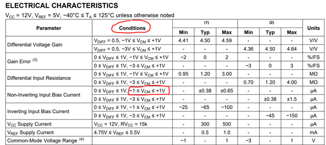
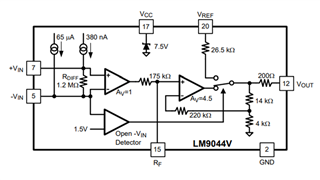
For the case of an open connection at the non-inverting input, the device would Show 2V due to The internal non-inverting input bias current 380 nA flowing through the differential input resistance(1.2M) but the IC output showing 4.8V.

I don't know why it is behaving like that .

We have measured the voltage and current  between inverting and non-inverting terminal in open condition it is showing 1.16V ( calculated current is 1.16V/1.6M =725nA) which is more comparable to the normal Ic (0.45V) (380nA)..

Please support for above issue ...

  • Hi Ajay,

    Can you include a schematic showing this circuit in more detail? 

    Was this device working, and then something changed, or this is a new device?

    Regards,
    Mike

  • Hi Ajay, 

    the IC output showing 4.8V

    Please provide the additional information and schematic per your application as Mike requested. 

    LM9044's Vout  at ~2V is estimated based on a typical O2 sensor's input impedance of 1.2MΩ. If I am taking the variations of the non-inverting input bias current, say ±0.65uA and 1.6MΩ, this will result in differential input voltage of 1.04V. If the differential_input_voltage*Gain of 4.64V/V, Vout = 4.826V in cold sensor or open input fault condition. 

    It is not conclusive to say that LM9044 IC is a failure case. Please provide us with the additional information. 

    Best,

    Raymond

  • During this high impedance condition the LM9044 will provide a default output voltage which 2V in cold sensor condition right ?

    Due to  internal non-inverting input bias current (380 nA typical) will flow through the differential input resistance (1.2 MΩ typical) and out the inverting input pin to ground. This will cause a voltage to be developed across the differential inputs:

    VIN(DIFF) = 380 nA x 1.2 MΩ VIN(DIFF) = 456 mV

    VOUT = VIN(DIFF) x 4.50

    VOUT = 456 mV x 4.50

    VOUT = 2.0V

    But is is always showing 4.8 V 

    For the case of an open connection at the non-inverting input, the device would react exactly the same as for the Cold Sensor condition.

    then why I am Getting 4.8V instead of 2V .

    In our Circuit We have some protection like short to battery ,sensor open .

    when input is open it has to show 2v but it actually showing 4.8 volt which Clash with short to battery indication (4.8v) controller is not able to decide either it is sensor open fault or short to battery fault .

    Pls give us solution so that in input open condition i will get 2V .


    one more addition point is that it is happening with only non inverting open condition not with inverting open condition .in inverting input open condition i am getting 2v which correct .

  • Pls find above circuit which i am using....

  • hey Michael,

    Pls find schematic in below chat .

  • In normal operation device working good only in non inverting open condition it is showing 4.8v instead of 2v

  • Hi Ajay,

    Thank you for providing your schematic and the additional information.

    During this high impedance condition the LM9044 will provide a default output voltage which 2V in cold sensor condition right ?

    The 2V output voltage calculation is the typical output voltage based on the typical Ib and input impedance specifications. The typical spec is based on the standard deviation of the part distribution, therefore the vast majority of the devices will be within this typical spec, but not all. The maximum specification covers 6 standard deviations, and many devices will show performance somewhere between the typical and maximum specification. As Raymond pointed out, it is possible for a device to show 4.8V output based on values that are within these device specifications.

    How many devices are showing this behavior?

    Based on your measurements, it seems that the input impedance is slightly higher than the typical value but well within the max, and the IB is near the maximum specification. Although for a differential voltage of 1.16V, the output should be over 5V even with the minimum gain spec. 

    Can you show the configuration that you used to measure the voltage and current between the input terminals? Because the non-inverting input is high impedance it is possible that connecting certain voltmeters to these nodes could add bias current or other errors that will reduce the measurement accuracy.

    one more addition point is that it is happening with only non inverting open condition not with inverting open condition .in inverting input open condition i am getting 2v which correct .

    The inverting open condition does not rely on the bias current or input impedance to provide a voltage output. Instead, an internal comparator switches the output to a resistive voltage divider that will produce an output of 2V when connected to a 5V reference voltage. Disconnecting both input pins should result in the output resistor divider. If you disconnect both input pins do you read ~2V at the output just like the inverting open condition?

    Thanks,

    Zach

  • hello sir ,

    thank u for your reply ..

    whatever you shared that i understood sir ..

    i want to understand why this input bias current is changing over the period of time if change then what is your solution to get 2V output at non inverting open condition.

    till now i am Having 10 sample in that i am getting 4.8 volt in open condition ..

  • Hello Zach, 

    1. When both inputs are open, the output is 2V as expected.

    2. Though the input bias current on non-inverting input and the differential input impedance are within datasheet specifications, when the board was tested for input open circuit condition as part of end of line tests, it showed 2V at the output and hence passed. it failed after approx. 2 months of usage. 

    3. I would like to understand how these values (bias current and differential resistance) vary over time.

    4. Can you propose any solution to modify circuit diagram for 2V in all possible conditions for input open circuit condition. 

    5. Can you propose any detection mechanism so that the variation could be minimized as part of End of Line tests.

  • Hi Ajay,

    I understand your devices passed the initial open-circuit test with a 2V output, and are now showing ~4.8V output for the non-inverting open condition. Do all 10 devices show exactly 4.8V or is there some variation between the device outputs? Can you measure the inverting input voltage and output voltage while the non-inverting input is disconnected? For this test the voltmeter cannot be connected to the non-inverting input, as this will close the pin.

    Do you have the data from the initial end of line tests? Were these done for all 3 possible open conditions: 1.) non-inverting open 2.) inverting open 3.) both open? Or was the test only performed for the condition of both pins open? Please provide the data if you have it available.

    I will consider your other points and try to come up with a solution, but I have a few more questions first.

    What is your ULS input voltage range? What voltage is applied to the non-inverting input when the connection is broken? Is the device powered on and biased to the input signal when the input is opened? Or is the input open before the device powers on?

    Thanks,

    Zach

  • Hi Zach,

    1)Do all 10 devices show exactly 4.8V or is there some variation between the device outputs--> All the 10 devices shows ~4.8-4.9V within this range..

    2)Inverting pin is connected to gnd.Via 100R 

    3)output voltage while the non-inverting input is disconnected-->4.8V

    4)we have tested it for only for the First case i.e non inverting open and the passing criteria is 2V ±0.5V .and it is not possible to test other cases as inverting pin is connected to gnd.

    5)ULS input range is 0.1v-0.8V.

  • Hi Ajay,

    Thanks for the information. Are you able to provide a layout of your board? Can you also provide a clear photo of your board showing the LM9044 and input connections? 

    I believe the best way to move forward is to take a few more measurements under two operating conditions. See below.

    1.) With the ULS_Input node connected to GND, use a high-impedance DMM to directly measure the following nodes:

    • Pin 5, -Vin
    • Pin 7: +Vin
    • Pin 12, Vout
    • Pin 15, Rf
    • Pin 17, Vcc
    • Pin 20, Vref

    2.) Repeat measurements above with the ULS_Input node floating.

    3.) With the ULS_Input node floating, connect oscilloscope probe to Vout and take scope capture. This is to ensure that the output is settling to a stable DC value and is not oscillating.

    Hopefully these results will give us a better understanding of what is happening in the circuit.

    Thanks,

    Zach

  • 1) With the ULS_Input node connected to GND, use a high-impedance DMM to directly measure the following nodes:

    • Pin 5, -Vin=0 Volt
    • Pin 7: +Vin=0 Volt
    • Pin 12, Vout=0 Volt
    • Pin 15, Rf=0 Volt
    • Pin 17, Vcc=12 Volt
    • Pin 20, Vref=5 Volt

    2) With the ULS_Input node floating, connect oscilloscope probe to Vout and take scope capture. This is to ensure that the output is settling to a stable DC value and is not oscillating.

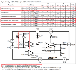
     == Its Showing pure Dc around 4.8Volt in input Floating Condition.

  • DMM impedance =10Mohm

  • Hi Ajay,

    For some reason I am not able to view the image of the scope capture, however I trust that you have verified a pure DC voltage at the output, thank you.

    Can you complete the DC voltage probes for the input open condition? I would like to compare with the input grounded condition.

    Can you provide the schematic showing the connections at the output of the device? What is connected at the ULS_uC pin?

    Can you test the input open condition with the ULS_uC node disconnected? What is the output voltage with only C7 connected to the output pin?

    Thanks,

    Zach

  • hello Sir,

    1)What is connected at the ULS_uC pin-->>> We have Mounted above schematic on General Purpose board to analyze the input open Condition so  ULS_uC is not connected anywhere at this pin we were checking opamp output only..

    2)Can you test the input open condition with the ULS_uC node disconnected----> 4.8V output

    3)What is the output voltage with only C7 connected to the output pin --->4.8V output

    Sir i request you to pls give some solution ….why IC behavior is changing over the period of time when Noninverting open condition happen ...initially it was showing 2 V but after period of time it is showing 4.8V....

  • Hi Ajay,

    Thank you for clarifying this. I will need to look into this further to determine a solution.

    I have ordered some LM9044 devices that I will test and attempt to replicate the behavior you are seeing. It may take some time to develop hardware to test these boards as this is an older device and we do not have an evaluation module developed.

    If you would like to send me some of your devices I can test them as well and use this as a comparison. If you are able to send one of your general purpose test boards along with the devices, this will help to get results quicker. If not I will need to develop a test board that can accommodate the unique package and this will take some additional time.

    Thanks,

    Zach

  • Hello Sir ,

    it is difficult to send Board but i just want to understand why Ic behavior is changing over the period of time ...

    pls take ur time to understand and hopes so, you will come up with a solution...

    thanks 

    Ajay 

  • Hi Ajay,

    Thanks, I will keep you updated on my results when I am able to test the devices.

    One more thing... Is the schematic you provided above the schematic for the general purpose board you are using?

    Can you provide a schematic of the board used in your application? I will need to see all the connections to the LM9044 as it operates in the field so that I can attempt to replicate the error. This includes the connections at the output of the device as it operates in the field. If you do not want to post the full schematic on this public forum, you may send it to me directly through a private message.

    Thanks,

    Zach

  • Hello Sir ,

    Sry for late reply .....

    Whatever Info i had that i have shared with you ..

    In the schematic only we are providing input range from 0.1V--0.8 v and observing  output accordingly.

    It is not possible to share complete schematic hope you will understand ...

    pls come up with solution so that in open input condition i will get 2 volt instead of 4.8 volt...

    Thanks 

    Ajay 

  • Hi Ajay,

    I will attempt to replicate the error with the information I have. I will keep you updated on my results when I am able to test the devices.

    Thanks,

    Zach

  • please find above attached screenshot of datasheet..

    As you said, the maximum specification covers 6 standard deviations, and many devices will show performance somewhere between the typical and maximum specification and it is possible for a device to show 4.8V output based on values that are within these device specifications.

    But according to the data sheet maximum open circuit output voltage is 0.423 x VREFF= 0.423 x 5 = 2.115V.

  • Hi Ajay,

    The max specifications for non-inverting input bias current and differential input impedance imply that an open circuit output voltage of 4.8V is possible based on the I*R.

    You are correct, that the open-circuit output voltage specification indicates a max of 0.423*5 = 2.115V but this is for a common-mode voltage ≤ 1V.

    If the floating inputs are somehow being pulled up to a common-mode voltage greater than 1V, this specification may not apply. I agree that under normal conditions, I would expect a maximum open-circuit output voltage of 2.115V.

    I was able to configure a test board with a fresh LM9044 in your circuit configuration and the open-circuit output voltage is ~2V as expected. For the next step, I would like to look at some of your devices in my test configuration to see if I can replicate the error.

    I will reach out to you in a private message to provide shipping address for these devices.

    Thank you for your patience while I have been developing the test board on my end.

    Regards,

    Zach

  • Hi Zach,

    How could the common mode voltage possibly be greater than 1V?

    As, it is mentioned in datasheet that maximum value of VCM is 1V. 

    please find below attached screenshot of datasheet.

    Regards,

    Ajay

  • Hi Ajay,

    The electrical characteristics datasheet contains the device specifications and the conditions under which these specifications are met. The min and max Vcm specification implies that this is the valid range in which the device is meant to operate. If the max Vcm specification is exceeded, the device may show performance outside of the specified range.

    Notice the "conditions" column for many of the LM9044 specifications require the Vcm to be less than 1V as part of the spec definition. The device specifications will only be met, if the required circuit conditions are also met.

    Notice there is also a condition of Vdiff <1V which according to your initial post, this condition is violated.

    We have measured the voltage and current  between inverting and non-inverting terminal in open condition it is showing 1.16V

    It is possible that something is driving the input past the valid range, which results in performance outside of the defined device specifications. This is could also be excessive leakage current into the high-impedance non-inverting input node, due to residual solder flux or other contaminants on the board. Are you able to clean the PCB especially around the device inputs? Do you see the performance improved after thorough PCB cleaning?

    I am in contact with the quality team regarding this issue. I will continue to update you on our progress.

    Thanks,

    Zach