This thread has been locked.

If you have a related question, please click the "Ask a related question" button in the top right corner. The newly created question will be automatically linked to this question.

OPA637: Transimpedance amplifier

Part Number: OPA637
Other Parts Discussed in Thread: OPA627

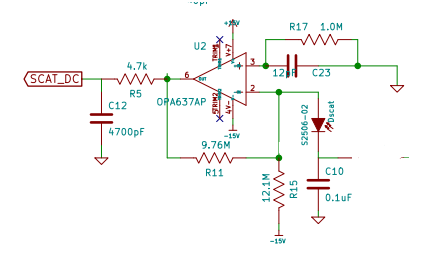
Attached below is the actual board design wth OPA637 with photodiodes
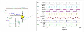
For testing purpose, I have removed photodiode from the practical circuit. I have taken jumper wires from the solder pads to feed input current from precision power source. Attached below is the simulation circuit and same goes for practical connections. 
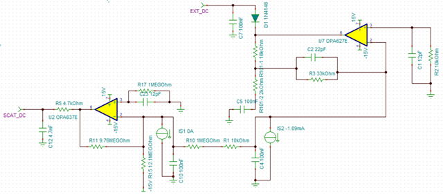
The input current fed is IS1=0A, IS2= -0.99mA to -1.60mA. Voltages observed for these corresponding input current values varies from -13.5V to 0.109V in practical.

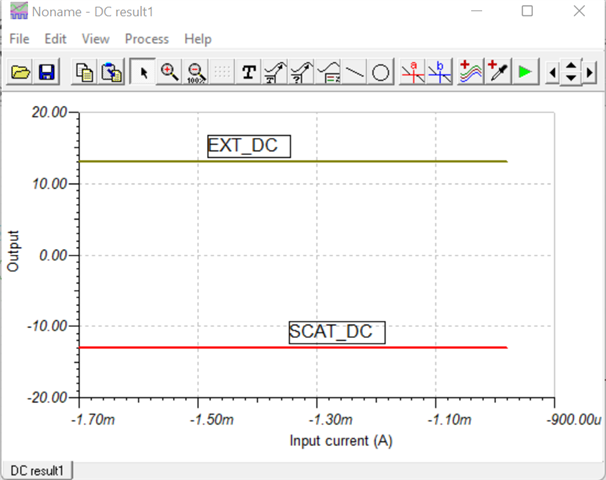
Whereas in simulation, I am getting voltage around -13.1V in these range. Attached image for reference.
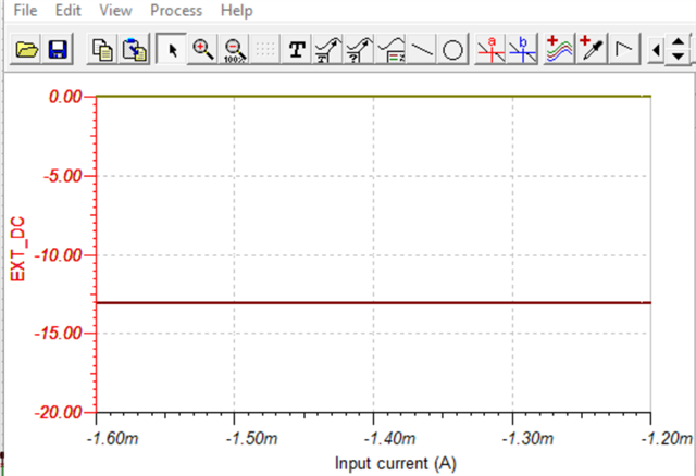
Kindly help on this.

  • Hi Nafisa, 

    The input current fed is IS1=0A, IS2= -0.99mA to -1.60mA. Voltages observed for these corresponding input current values varies from -13.5V to 0.109V in practical.

    You need to provide us what or how the circuit is functioning, other than it will perform I-to-V conversion. For instance, what are two photodiodes for? What do they measure, UV-VIS-NIR or something else? What are the time and BW response of the photodetectors? Is one photodiode referenced to other one, say it is detecting an ambient light conditions?

    OPA637 TIA 05262023.TSC

    Anyway, I simplified the circuit and I see that the circuit's linear response range is from -350uA to 406uA for Vout2. If you see -13V at the either output (Vout1 or Vout2), the OPA637 is already reached saturation. You need to explain what the application is, so that we can provide you additional suggestions or recommendation. 

    Best,

    Raymond 

  • Attached block diagram for the board working

    Photodiodes part number S2506-02

  • Hi Nafisa,

    I see what is the application. 


    I have a question. Are there requirements to link two photodiodes with 1MΩ and 10kΩ? I'd like to know the reasons behind the configuration. 


    If I understood the attached block diagram correctly, you'd like to measure the scattered transmittance angles of the liquid that going through the flow cell. You will get the liquid characteristics from the refractive angle measurement, By knowing the refractive angle, the reflective index of the liquid may be calculated. 

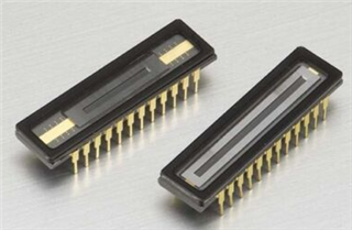
    Typically, this type of setup is measured via CMOS linear image sensor, where the sensor placement and alignment are very precise. The example of such measurement is similar to optical spectrometer, where light intensity from UV to NIR is measured (say with 512 or 1024 sensor or pixels of a linear array). Your setup may work as is, but the optical alignment, optical jig and light calibration may be more difficult to obtain from the discrete photo receivers.   

    Back to the inquiry, my understanding is that all photodiodes' current are monitored independently. There should not be photodiode connection from the light receivers. Laser is the incident light source, and light scattering and refractive characteristics are measured independently at the light receivers. The current-to-voltage conversions are sampled and monitored independently.

    You may sum the output current after the light receivers' current are amplified and converted, but light receivers' signal maybe treated separately. You may have to go through I-to-V converters since the light receivers' signals can be very weak. 

    If your flow cell is using cuvette or square or rectangular shape apparatus, the laser source likely have to go through a slit. On the light receiver side, there may be also implemented with a slit and/or with optical narrow band filters. With the large area of the photo detector (2.77x2.77 mm^2), the light incident angles may be too wide, where you may not be able to achieve the intended optical effects from the measurement. 

    Anyway, if you have additional questions, please let us know. 

    Best,

    Raymond 

  • Hi,

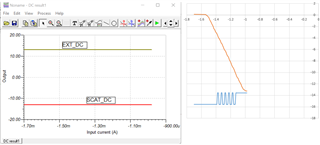
    1. Attached simulation and practical results for the SCAT_DC and EXT_DC outputs with input given only to the diode DEXT in the range of -0.98mA to -1.7mA. Both results are not similar.

    EXT Diode(mA) SCAT_DC(V) EXT_DC(V)
    -0.98 -13.576 -13.218
    -0.99 -13.582 -13.231
    -1 -13.582 -13.165
    -1.01 -13.582 -13.08
    -1.02 -13.581 -12.995
    -1.03 -13.581 -12.905
    -1.04 -13.58 -12.651
    -1.05 -13.58 -12.445
    -1.06 -13.58 -12.072
    -1.07 -13.58 -11.845
    -1.08 -13.58 -11.618
    -1.09 -13.58 -11.372
    -1.1 -13.58 -11.034
    -1.11 -13.581 -10.881
    -1.12 -13.58 -10.654
    -1.13 -13.58 -10.296
    -1.14 -15.581 -9.992
    -1.15 -15.581 -9.648
    -1.16 -15.581 -9.339
    -1.17 -13.58 -9.123
    -1.18 -13.58 -8.923
    -1.19 -15.581 -8.618
    -1.2 -15.581 -8.256
    -1.21 -15.581 -8.012
    -1.22 -13.58 -7.763
    -1.23 -13.58 -7.365
    -1.24 -15.581 -7.17
    -1.25 -15.581 -6.984
    -1.26 -15.581 -6.651
    -1.27 -13.58 -6.322
    -1.28 -13.58 -6.142
    -1.29 -15.581 -5.954
    -1.3 -15.581 -5.616
    -1.31 -15.581 -5.335
    -1.32 -13.58 -5.01
    -1.33 -13.58 -4.882
    -1.34 -15.581 -4.54
    -1.35 -15.581 -4.275
    -1.36 -15.581 -4.072
    -1.37 -13.58 -3.856
    -1.38 -13.58 -3.506
    -1.39 -15.581 -3.216
    -1.4 -15.581 -3.045
    -1.41 -15.581 -2.855
    -1.42 -15.581 -2.518
    -1.43 -15.581 -2.379
    -1.44 -15.581 -1.99
    -1.45 -15.581 -1.732
    -1.46 -15.581 -1.487
    -1.47 -15.581 -1.196
    -1.48 -15.581 -0.992
    -1.49 -15.581 -0.732
    -1.5 -15.581 -0.41
    -1.51 -15.581 -0.281
    -1.52 -15.581 -0.117
    -1.53 -15.581 -0.067
    -1.54 -15.581 0.09
    -1.55 -15.581 0.098
    -1.56 -15.581 0.102
    -1.57 -15.581 0.104
    -1.58 -15.581 0.105
    -1.59 -15.581 0.107
    -1.6 -15.581 0.109
    -1.61 -15.581 0.115
    -1.62 -15.581 0.116
    -1.63 -15.581 0.12
    -1.64 -15.581 0.121
    -1.65 -15.581 0.122
    -1.66 -15.581 0.123
    -1.67 -15.581 0.126
    -1.68 -15.581 0.131
    -1.69 -15.581 0.134
    -1.7 -15.581

    0.137

    2. With regard to your query on requirements to link two photodiodes with 1MΩ and 10kΩ, this is legacy board design. So we also don't have any idea on this circuit.

  • Hi Nafisa,

    the SCAT_DC and EXT_DC outputs with input given only to the diode DEXT in the range of -0.98mA to -1.7mA. Both results are not similar.

    I am not sure that what I am looking at. The presented graph and attached results are different. Should EXT_DC and SCAT_DC have the same result?

    Regarding to OPA637, the system is operated near op amp's saturation region. The OPA637's linear region is within ±11V in ±15V supply rails. So I do not know why you are looking at and comparing the results in the saturation region, which it has little meaning for the application. 

    Are you trying to understand the legacy optical design in the application? 

    If you are trying to duplicate this optical setup, the optical apparatus is just as critical to the photopic detections. The laser is emitting directional and collimated light source, and PD2 is direct transmittance receiving signal, which its light intensity should be much stronger than PD1. In addition, the laser beam has a collimated lens in front of the emitter. If you do not have the correct optical setup, you will never get what the intended design and effects of the measurement. In addition, the laser emitter's light intensity is a huge variable, and it seems like that your I-to-V converter is operating in saturation mode. 

    You need to adjust the optical system, where light receivers are operating in I-to-V linear mode. So you need to adjust the optical system that the photo detectors are operating in a linear mode, otherwise, you will not get what you are looking for.  

    If you have additional questions, please let me know. 

    Best,

    Raymond

  • Hi

    Thanks for your response.

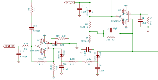
    I have a question regarding the below circuits.

    How can I do simulation If I want to know the behavior of these two circuits? Like, removing photodiode and instead using current source is one of the ideas. Is there any other method to understand this circuit with T-network?

    Matching simulation results with opamp calculation is the ultimate goal.

    Kindly help on this.

  • Hi Hi Nafisa,

    How can I do simulation If I want to know the behavior of these two circuits?

    Could you tell me how the photo detectors are triggered in the setup? I need to know how the circuit is operating. Picture would help. What does the circuit design to do?

    From the optical light measurement point of view, light scattering measurement on the receiver side are totally independent optical measurement. I do not know why the designer linked two receivers together.  

    You would have to simplify the two circuits and configured it in the simulation to see what the previous designer is intended to do. I can simulate two circuits in Tina, but I am unable to tell you what the designer's intend. So you would need to provide me with more details, such as timing of the light measurement, light pulse duration from laser, what is laser diode and output voltage relationships etc.. It seems that these setup is light pulsation optical measurement. 

    Best,

    Raymond

  • Hi Raymond,

    This board is a particle sizing detector which uses laser diode. When the laser light is allowed to pass through the flow cell, some light gets absorbed and some gets scattered by the particle in the flow cell. So, the scattered light is captured by SCAT diode and the absorbed light is captured by EXT diode and these diode outputs are fed to the trans-impedance amplifiers. And then, both the opamp outputs are sent to a summing amplifier and based on that output, pulse is generated. This pulse height gives the size of the particle. This is the overall functionality of the setup.

    So, here this opamp and photodiodes are integrated into a single PCB, and I am working on simulating these circuits.

    Note: The output of the photodiode will be proportional to the input light, so constant light would produce a DC signal, and oscillating light would produce an oscillating signal (i.e. particle detected stage). 

    As this is legacy board design, we also don't have any idea on this circuit. In bench testing, we have isolated the PCB from the laser setup and also removed photodiode as there is no laser diode to provide inputs to it. Instead, we are giving current inputs (because photodiode output will be current) to the opamp and trying to analyze the SCAT and EXT_DC opamp section.

    My main aim is to find out the response of these SCAT_DC and EXT_DC section. As, this is a trans-impedance amplifier with T-network configuration, I am trying to match the simulation results for these both sections with the calculation (trans-impedance T-network formula). I have tried to calculate the output with T-network formulas provided in TI website but still couldn't match both the results. So, please provide your suggestion to achieve this scenario like matching simulation and calculation results.

    Regards

    Nafisa

  • Hi Nafisa,

    Thanks for the explanation. I am starting to understand what the designer is doing. Please consider this as discussion, since you would need to test data and verify what I am saying below. 

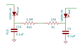
    Consider particles in a liquid is moving at certain pace, and the light detector is seen scatter reflection from particles and generate the "pulsation" current as shown in the simulation. The capacitor will charged up due to the pulsation current waveform and seen by SCAT_DC. Since there is 4.7k and 4.7nf LPF, the measurement events are <7.2kHz, likely <700Hz range (the motion of particle in a liquid should be slow). In addition, the liquid is moving in a flow cell, therefore, the SCAT_DC may look like what is simulated below. SCAT_DC signal is weak, and it may look like a DC biasing with a DMM. You may have to  measure it with scope to capture the scattering effects.  

    OPA637 E2E Scattering 07072023.TSC

    The OPA637 is uncompensated amplifier and it won't be stable unless Gain > 5V/V. The original design may use OPA627 instead, which is stable. 

    In terms of this circuit below, it may be designed as a pi filter. I have no ideas. If you remove the resistor link, would the circuits behave the same? 

    From the optical measurement point of view, one should not "link" between the transmittance light intensity and scattered light intensity. These are two independent events. The two light intensity measurements may be proportional, but I do not understand why the designer links the detectors in this manner. 

    I will get other simulation going when I have a chance. Please let me know if this is helpful.

    Best,

    Raymond

  • Hi Nafisa,

    I have a question. I need you to capture the actual photodiode waveform and current level in order to understand what it is going on. 

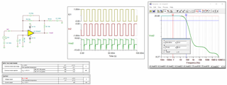
    If I simulate the diode waveform in square wave from 0 to 1mA @100Hz, I see the following response. But there is a problem, OPA627 is unable to provide a linear output response per the datasheet, so is the above simulation, see the simulation below. The circuit is operated at the edge of the op amp's linear responses. 

    If I assumed that the above configuration, then the frequency BW of the system is even lower, -3dB is approx. 80Hz. Are you sure that the photo sensor is placed in the direction shown in the schematic? As is, the gain is only 63V/V (36dB) and the application does not need to use T-Network configuration. 

    OPA627 TIA 07082023.TSC

    Does the particle size measuring system working? Have you checked with the calibration of the particle size measurement system?  And How it is calibrated?

    I do not know the history of the apparatus. Typically, you should check the system with a known particle distribution mixture presented in the flow cell. That is how you should verify if the measurement is working per the application. This is a fairly complicated optical measurement system. Yes, the theory may be simpler, but the optical and electronic implementations are not so easy.  

    Best,

    Raymond