Hi Team,
Could you help with the follow question from Samsung.
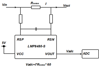
1. The LMP8480 device is powered by 5V. Under normal conditions, Vadc is less than 5V. However, in some cases, an increase in current can cause the differential input I*Rsense*60 of the LMP8480 to exceed 5V. In this situation, will the output of Vadc be clamped at 5V max? Will there be overvoltage stress on the IN+/- pins? If so, how can this problem be resolved?
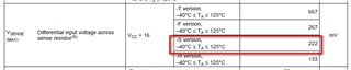
2. The figure below shows the range of Vsense when VCC=16V. Will the range be the same when VCC=5V?
3. The figure below shows the margin between Vout and VCC when VCC=4.5V and Vrsp=48V. Will the parameters be the same when VCC=5V?

BR
Adrian