This thread has been locked.

If you have a related question, please click the "Ask a related question" button in the top right corner. The newly created question will be automatically linked to this question.

JFE2140: Offset Correction Integrator Circuit in JFE2140EVM

Part Number: JFE2140
Other Parts Discussed in Thread: , OPA202, OPA145

Hi,

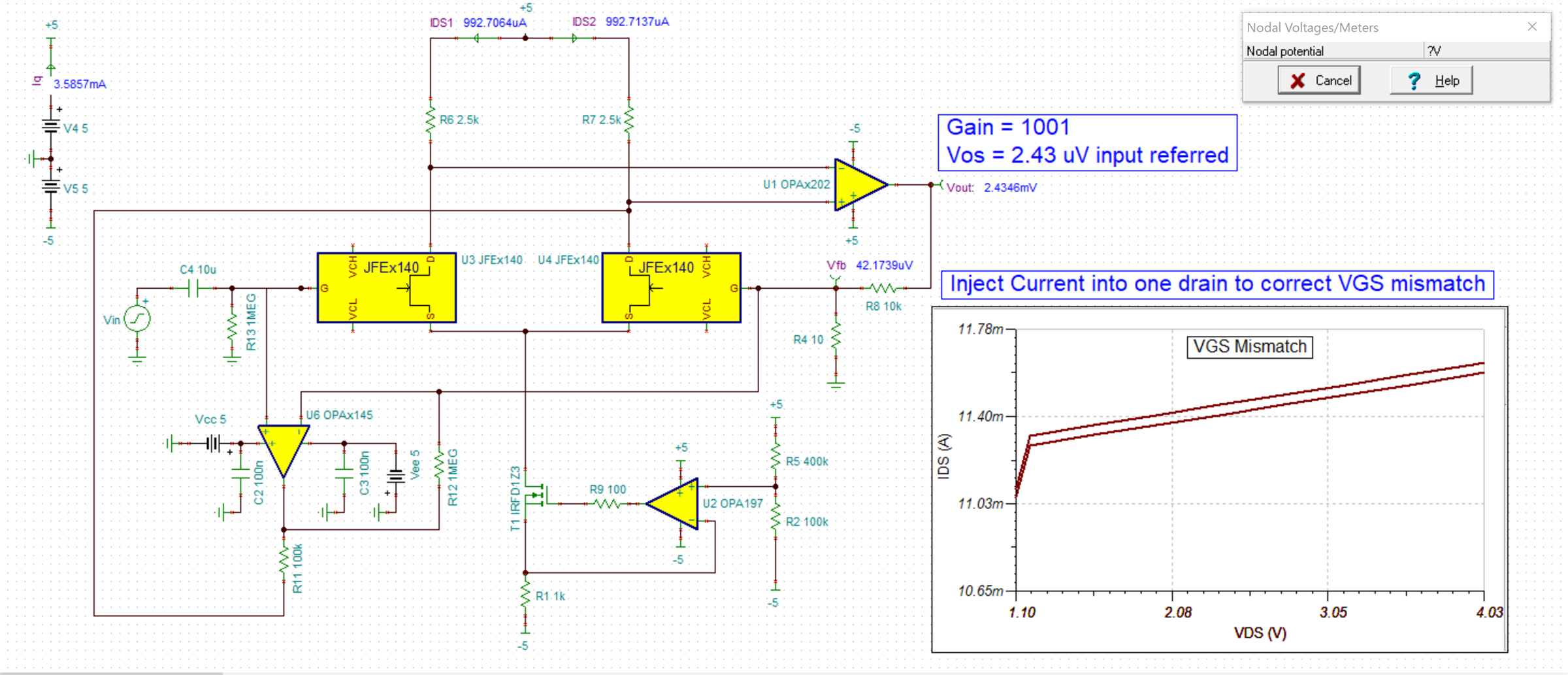
Is the offset correction integrator circuit (U3 & surrounding) in the JFE2140EVM actually tested working?

https://www.ti.com/lit/ug/slpu010/slpu010.pdf

I've run a simulation with the offset correction integrator circuit inserted & it doesn't work.

  • Hello, 

    I tested and did an extensive study on the integrator. It will work to correct the offset voltage, however I have found that it adds the noise of the amplifier used to do the correction and defeats the purpose of using the circuit as an ultra low noise amplifier. I put it on the board originally and had it apart of the published JFE2140 app note. I removed it due to the noise that it added. I still have simulation files that show it working as a correction circuit. You have to be careful with component values in order to get it to work. such that the resistor that is on the output of the amplifier connected to the drain is not to small such that it re-biases the JFET away from it's intended operating point or that it is too large and cause the correction amplifier to rail out. 

    Best Regards, 

    Chris Featherstone

  • Hi Chris,

    Thanks for the input, and I agree with your comment. By having 2 circuits driving the same summing point of the driver amplifier (U1, OPA202), the noise of the offset correction integrator become dominant.

    However, I still like the idea of having an offset correction integrator to monitor and correct the offset at real time, perhaps I could sum the accumulative offset voltage at a later stage of the amplifier.

  • Hey Chia, 

    Here is a screen capture of one of my experiments. I changed one of the JFET models by adjusting the VTO parameter by 2 mV to have a mismatch between the two JFET models in Tina Ti. The circuit reduces the input mismatch of 2 mV down to 2 uV. 

    Testing this on the EVM I was able to correct the mismatch as shown below. 

    Best Regards. 

    Chris Featherstone

  • Hi Chris,

    This simulation circuit is different from the circuit in https://www.ti.com/lit/ug/slpu010/slpu010.pdf, where the feedback of the U6 (OPA145 offset correction monitor) is not really an integrator but rather an "almost" open-looped op-amp. I will try it again with these value. Thanks.

  • Hey Chia, 

    Yeah, it was originally meant to be an integrator. As I experimented more and learned more in depth I started to modify the configuration. I left a bunch of footprint options on the pcb in order to experiment with. Best of luck!

    -Chris Featherstone

  • Hey Chia, 

    I did some digging around and found the simulation for convenience. 

    JFE2140 Vos Correction Circuit.TSC

    Best Regards, 

    Chris Featherstone