This thread has been locked.

If you have a related question, please click the "Ask a related question" button in the top right corner. The newly created question will be automatically linked to this question.

INA181: Current sense amplifier circuit recommendation

Part Number: INA181

Hello,

Looking for a validation of the circuit attached or a recommendation to improve further.

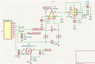
The picture shows a circuit using INA181 and TLV9001IDCK to sense current through a 12V battery. Pins 1 & 2 on terminal block J1 is a battery connector. The pin number 1 is the battery positive supply where a p-channel MOSFET is configured to protect the load from reverse polarity and pin number 2 is the battery negative supply where the INA181 is configured across a 10 milli ohm resistor for current sense.

Please have a look at the schematics attached and let me know your thoughts.

Thanks,

  • Hello Mahboob,

    I would say if you do not expect much noise in current is you do not need to have the R17 and R19.  This will reduce errors seen by IB.  Also the load at the output of INA181 is not shown.  Make sure if there is a capacitor it is under 1nF and if it is connected to a SAR ADC then look at this application report.  https://www.ti.com/lit/an/sboa443/sboa443.pdf

    Regards,

    Javier

  • Hi Javier,

    Thank you for your response.

    Most of the time a 12V battery will be used in this application but there are times a AC-DC converter is also used on this product which I think will bring in a lot of noise so I am planning to keep R17 and R19. Should I go for a lower valued resistor instead or 10ohms is fine? 

    You are right, a 12bit SAR ADC is used here. We have had noise issues in the past so, I was thinking of adding an RC filter at the output of INA181. Would you recommend the value of this filter as R=100ohms and C=10nF?

    Appreciate the help.

  • Hello Mahboob,

    The R17 and R19 should not go above 10Ω as the bias current will create a larger error.

    The RC is normally defined by the ADC and the conversion time and sampling time.  Normally the default reply for the capacitor size is 20x the sampling capacitor of the ADC.  ADC sampling caps are normally in the tens of pF.  The reason the capacitor size is 20x the sampling capacitor is some of the charge for the ADC to come from the capacitor but then charge up fast enough for the next sample.  This is if you need the fastest sampling.  I am sure you can find more information https://www.ti.com/video/series/analog-to-digital-converters-adcs.html I would look at  

    Section: Successive-approximation-register (SAR) analog-to-digital converter (ADC) input driver design (7)   

    Videos : Introduction to SAR ADC front-end component selection,  Math behind the R-C component selection

    If you don't need to sample fast then you may not need this.  If you are going above 1nF I would recommend above 500Ω due to the output impedance I see on the datasheet so you don't have stability issues.

    Regards,

    Javier