This thread has been locked.

If you have a related question, please click the "Ask a related question" button in the top right corner. The newly created question will be automatically linked to this question.

INA2331: Offset setting issue for custom circuitry for 10mV to 100mV range in single supply operation of INA2331

Part Number: INA2331
Other Parts Discussed in Thread: INA331, TINA-TI, LM27762, AFE5816, OPA325

Hi

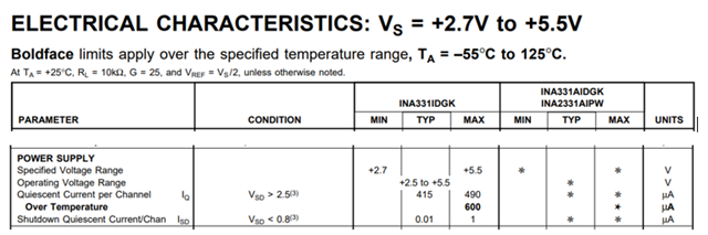
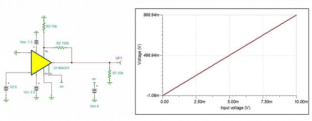
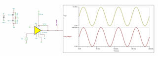
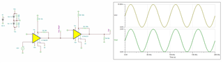
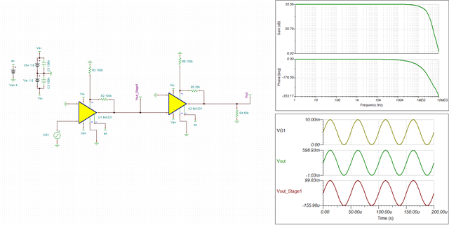
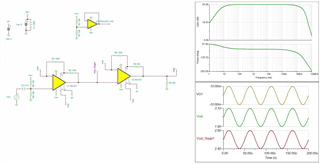
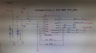
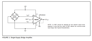
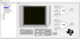
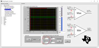
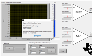
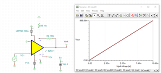
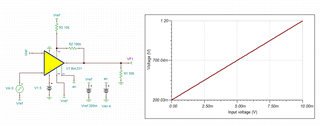
I'm implementing below circuitry for amplifier section. The input signal voltage will range between 10uV to 10mV. But in the current circuit, the offset is set by feedback circuit which i observe as not working. When a 1 mV signal is given with less than 3mV offset, output is getting clipped. Vref pin is not connected to any external voltage.

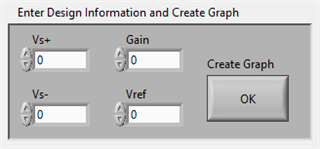
I would like to connect the external voltage to increase input offset such that a gain between 100-200 can be set for the input 1mV signal.  Suggest modification to be done for the same. Will giving Vref voltage result in amplification of that offset voltage also.

Can i set offset by connecting capcitor to ground for Vref pin, if so what should be minimum value of capacitor.

  • Hi Bivin,

    I see you have vin- connected to ground, and vin+ is a signal between 10uV and 10mV. In this case you are violating the valid common-mode input range of the INA2331.

    When operating on a single-supply, the INAx331 is designed to interface with small differential voltages riding on a common-mode voltage that satisfies the input requirements. Similar to figure 2.

    The "INA Vcm vs Vout" tool in the Analog Engineer's Calculator is a useful tool for determining valid common-mode, differential input, and output swing for various TI INAs.

    This TI Precision Labs video explains how to use the Analog Engineer's calculator to generate the boundary plot for 2-amp INAs such as INA331:  ti.com/video/6261788032001

    For the circuit shown, if you are able to use split supplies (+/- 2.5V) you will be free to operate at a common-mode of ~0V.

    If split supplies are not available, I can help you to determine another solution.

    Can you specify some of your design requirements?

    What is the application?

    What is the input signal and/or sensor?

    Will giving Vref voltage result in amplification of that offset voltage also.

    The gain from the Vref pin to Vout is +1V/V. The Vref voltage will not be amplified by the circuit.

    I notice there is a TINA-TI Reference design available to simulate the INA331. This along with the Analog Engineer's Calculator can be very useful to design and verify your circuit in simulation.

    sboc173b.tsc

    Thanks,

    Zach

  • Hi Zach

    Can you suggest the minimal modification on this circuit that can be done to support single supply operation as well as input signal of above range (between 10uV and 10mV). As per your comment, if Vref pin voltage is set to 200mV, then will an input signal of 1mV Vpp (with Vp of 0.5mV & Vn of -0.5mV) gets amplified.

    I was not able to choose the option using Tool provided, it was showing below error. I'm not able to set value. Provide steps to be followed.

    Page not found error is observed for below.

    "This TI Precision Labs video explains how to use the Analog Engineer's calculator to generate the boundary plot for 2-amp INAs such as INA331:  ti.com/video/6261788032001 "

    Thanks

    Bivin

  • Hi Bivin,

    The INA tool wants you to set a valid power supply voltage and a Vref voltage within the power supply range.

    If this error comes up, you may simply click "ok" and then continue to set the Vs+, Vs-, and Vref values until the operating voltage range is satisfied.

    Sorry for the broken link, this one should work: https://www.ti.com/video/6261788032001

    Can you suggest the minimal modification on this circuit that can be done to support single supply operation as well as input signal of above range (between 10uV and 10mV).

    I see two options to meet your design requirements...

    One option is to find another amplifier that allows a common-mode input voltage below the negative rail. These "ground sense" devices are common for low-side current measurement. Is your application a low-side current measurement sensing the voltage across a shunt resistor?

    The second option if you prefer to use the INA2331 with minimal circuit modifications, is to generate a small negative bias for the negative rail which will allow a true 0V common-mode input voltage. The LM7705 is a negative bias generator that produces a -232mV bias and can be operated directly off your existing 5V supply. See below.

    Thanks,

    Zach

  • Hi Zach

    The two suggested solution requires modification of PCB by adding new IC or by modifying existing amplifier.

    To make the above circuitry to operate using single supply, will connecting Vref pin to a 200mV voltage fix this issue.

    Regarding tool,i'm still getting same error. The RED circled portion is your input screenshot.

    Thanks

    Bivin

  • Hi Bivin,

    Unfortunately I am not able to see your screenshot. You can try to copy and paste the image into the message, this usually works for me.

    To make the above circuitry to operate using single supply, will connecting Vref pin to a 200mV voltage fix this issue.

    Apply a 200mV reference voltage will not extend the valid common-mode input range to the negative rail. The purpose of the reference voltage is to set the zero output voltage level. The common-mode input voltage must still be considered, as in the equation below.

    In fact, increasing the reference voltage will increase the minimum common-mode input voltage range.

    See in the boundary plot that with Vref=200mV, the minimum Vcm is 59mV with almost no dynamic range.

    Are you able to bias your input source with the same reference voltage? See in the simulation below, with both inputs biased to the 200mV reference voltage, the device is in linear operation for the input differential voltage of 10μV-10mV and the input common-mode voltage is satisfied at 200mV.

    The output is defined by the following equation: Vout = Vref + G*(Vin+ - Vin-)

     0

    INA331_Vcm_Bias.TSC

    Regards,

    Zach

  • Hi Zach

    I'm having total of 18 INA2331 amplifier and can you suggest the best ultra low noise inverter with LDO IC which supports all 18 biasing. In case of updating the circuit, can you share a sample circuitry on how the connections to be updated for existing circuit shown above in the question.

    Consider +-3.3V biasing for the IC.

    Can i use LM27762 for biasing, will 18 INA2331 be supported using the same ? Maximum how many of this can be supported ?

  • Hi Bivin,

    I will forward this to the team that supports LM27762, they will be able to provide the appropriate recommendation.

    Please let me know if you require further support with the INA2331 device.

    Thanks,

    Zach

  • Hi Zach

    What will the maximum bias & operating current required for single INA2331 IC.

    Do you have any suggestion for LDO, is LM27762 good enough to support INA2331 noise requirements ?

    Thanks

    Bivin

  • Hi Bivin,

    is LM27762 good enough to support INA2331 noise requirements

    I will check the INA2331 specs and get back to you tomorrow.

    Regards,

    Febin

  • Hi Bivin,

    What will the maximum bias & operating current required for single INA2331 IC.

    As shown in the electrical characteristics section of the datasheet, the maximum operating supply voltage (Vcc-Vee) is 5.5V and the maximum IQ over the temperature range is 600μA.

    Consider +-3.3V biasing for the IC.

    From these specs, it is clear that you cannot operate at +/-3.3V. However, you may operate using asymmetrical supplies such as +3.3V and -1.5V.

    I will let Febin comment on the LM27762 or other LDO recommendations for driving 18 INA2331 devices.

    Can you tell us what is your signal bandwidth?

    Thanks,

    Zach

  • Hi Bivin,

    One quick correction, the INA2331 specifies a max IQ over temperature of 600μA per channel. Which means that the max IQ over temperature for the dual channel INA2331 is 1200μA. This will be important when determining the power budget of your LDO.

    Regards,

    Zach

  • Hi  

    Consider signal bandwidth as 2MHz & operating voltage as +-1.8V. What could be the maximum gain possible, can you share a circuitry for the same.

    Regards

    Bivin

  • Hi Bivin,

    The maximum output voltage for INA2331 with +/-1.8V supplies is 0.6V. I believe your design is targeting a 2V output? In this case, a positive rail of 3.3V is required as this will allow a max output voltage of 2.1V. The negative rail may be anywhere between -200mV and -1.8V to accommodate the ~0V common-mode input signal.

    Consider signal bandwidth as 2MHz

    According to the datasheet, INA2331 has a -3dB bandwidth of 2MHz in a gain of 25 V/V.

    The bandwidth of a voltage-feedback amplifier is inversely correlated to the gain applied. See from INA2331 gain vs frequency curve, the -3dB bandwidth in a  gain of 100 V/V is ~350kHz.

    In order to satisfy your bandwidth requirements, the total gain of 200 V/V should be split more evenly between the two stages. A gain of 20 V/V for the first stage and a gain of 10 V/V for the second stage should suffice.

    See common-mode input, differential input, and Vout max for the first stage configured in a gain of 20 V/V.

    See output of first stage.

    The input and output limitations of the second stage must also be considered as the common-mode input voltage has changed from ~0V to 100mV, and the differential voltage has increased to 200mV. Notice the Vin+ (max) for the second stage is 205mV, our signal is just within this range at 200mV!

    See the 2V output is achieved.

    8836.INA331_Vcm_Bias.TSC

    Regards,

    Zach

  • Hi Zach

    Can you share a schematic PDF which operates with +-1.8V.  Maximum gain can be considered for 0.6V output with 10mV input signal .

    Please reply on LDO query.

    Regards

    Bivin

  • Hi Bivin,

    LM27762 is a charge pump with integrated LDO for each output rail. 

    From what I understand, you may want to power 18 INA2331 devices from a single LM27762.

    From the d/s, output ripple increases with output current. Depending on the total load you want to drive with a single LM27762, we can approximate the ripple from this graph.

    Doing some rough calculations, looks like it is hard to achieve the input noise requirements of INA2331 with LM27762. Unfortunately, this is the only dual Charge pump with integrated LDO in our portfolio. If you need an LDO specifically, I can re-direct to the LDO team.

    Bdw, what is the application? 

    Regards,

    Febin

  • Hi Bivin,

    See below schematic for +/- 1.8V supplies Maximum gain is 60 V/V for 10mV input signal.

    See attached TINA schematic for your reference.

    INA331_1.8Vsupplies.TSC

    Regards,

    Zach

  • Hi Zach

    Thanks for sharing files.

    Regards

    Bivin

  • Hi Febin

    Share details of a power supply LDO topology which support 18 INA2331 IC with +-1.8V bias from a single 12V or 5V input along with ripple requirements.

    Can you share an estimate of maximum current requirement for 18 INA2331 IC.

    Regards

    Bivin

  • Hi Bivin,

    Zach will take lead for this thread. 

    Regards,

    Febin

  • Hi Bivin,

    The max IQ over temperature is INA2331 is 600μA per channel. For 18 devices, the IQ requirement is 600μA x 2 x 18 = 21.6mA. Note this is just the quiescent current requirement and you will still need to supply the necessary current to drive your load, which is not shown in your schematic. What is the output current requirements for your INA2331 circuit? Can you provide a schematic showing the load?

    The LM27762 supplies up to +/-250mA which may be enough to supply 18 devices, depending on the loading condition. As Febin showed in his post, the voltage ripple increases with output loading of the LM27762 and is on the order of mV. In order to resolve input signals in the mV range, this voltage ripple should be suppressed by an additional LDO stage with appropriate filtering.

    I can reach out to the LDO team on your behalf for an LDO recommendation. Please share the output current/loading requirements of your circuit so I can recommend the proper solution.

    Thanks,

    Zach

  • Hi Zach

    I'm using this as a preamplifier for AFE5816 IC. You may consider the load current based on AFE IC input requirement.

    In case you suggest additional LDO for +-1.8V generation , you may suggest a dual output regulator with improved current output instead of LM27762 to improve efficiency & reduce power dissipation.

    Regards

    Bivin

  • Hi Bivin,

    I see AFE8516 is for ultrasound applications. Is this an AC application? If so, you may simply AC couple the input and apply your own mid-supply common-mode voltage directly at the input pin of the INA2331. This will satisfy the DC common-mode input requirements of the INA while using the single 5V supply. See circuit below and attached TINA simulation.

    INA331_Vcm_Bias_AC_Coupled.TSC

    As shown in the image above, you will need to apply 2.5V to the ref pin and the Vin+ pin for both stages of INA2331. This reference voltage must be low-impedance for the entire signal bandwidth. If you do not have a low-impedance 2.5V reference available, I recommend using OPA325 as a reference buffer as shown in the circuit above.

    This will be the preferred solution as it is unlikely we will be able to produce a dual supply charge-pump/LDO solution that will meet the given performance requirements.

    Regards,

    Zach

  • Hi Zach

    I have to operate IC at 3.3V with 10mV maximum input voltage. Can i set vref/-IN/+IN pin voltage as 0.33V (1/10th of 3.3V). Rest of the circuitry remains same.

    Input & output will be AC coupled .

    Regards

    Bivin

  • Hi Bivin,

    You cannot set Vref to 0.33V as this does not allow enough common-mode range for your input and output signal.

    For a 3.3V supply, it is optimal to apply a 1.2V reference and 1.2V common-mode voltage as this will allow the widest input and output swing.

    This can be achieved with the same circuit shown in my previous post by adjusting the resistor dividers.

    Regards,

    Zach

  • Hi Zach

    Thanks for the support.

    Regards

    Bivin

  • Hi Bivin,

    No problem, I'm happy to help.

    I will go ahead and close this thread. Feel free to reply again if you require further support on this issue.

    Regards,

    Zach