Because of the holidays, TI E2E™ design support forum responses will be delayed from Dec. 25 through Jan. 2. Thank you for your patience.

This thread has been locked.

If you have a related question, please click the "Ask a related question" button in the top right corner. The newly created question will be automatically linked to this question.

LM2904B-Q1: temperature drift

Part Number: LM2904B-Q1
Other Parts Discussed in Thread: LM2904LV-Q1, LM2904, LM2904-Q1,

Dear team,

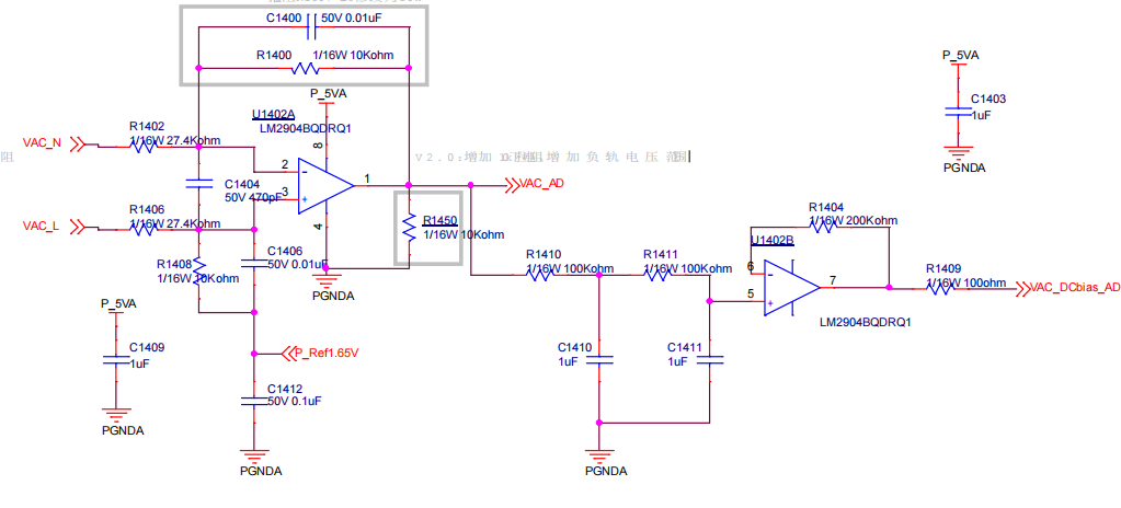
My customer found that in low temperature environment (-40℃), AC sampling has a large deviation, about 7V; room temperature and high temperature in the deviation of about 2V. Could you please help analyze why the deviation is so large in the low temperature?

Application condition: Vo=Vac_AD=V_P_Ref1.65V+0.0033*1.414*Vac; Io=Vo/10k; according to the computation, the average output current is 0.16~0.2mA.
In my understanding, below spec means that the minimum output voltage is (V-)+20mV. For example, if (V-)=0V, then the minimum value should be 20mV in the worst case, right?

Thanks & Best Regards,

Sherry

  • Hi Sherry,

    I'm a little confused that the customer is seeing a 7V AC deviation while the op amp is on a 5V supply. 

    Some questions I have: 

    • What does the customer define as AC deviation?
    • Do they have any screenshots?
    • I'd like to know what the input signals are of VAC_N and VAC_L? 
    • Is the problem occurring at VAC_AD or VAC_DCbias_AD? 

    I need to get a better idea of what is happening before I can determine what the root cause is. 

    Best Regards,

    Robert Clifton

  • At low temperatures, the limit of the input common-mode range is lower. I suspect that one of the input voltages at pins 2/3 goes above 3 V.

    If this is the problem, use the LM2904LV-Q1 instead, which has a wider range, up to (V+) – 1 V.

  • Hi Ladisch,

    The customer feedbacks that the maximum voltage at pin2/3 is around 2.9V.

    Thanks & Best Regards,

    Sherry

  • Hi Robert,

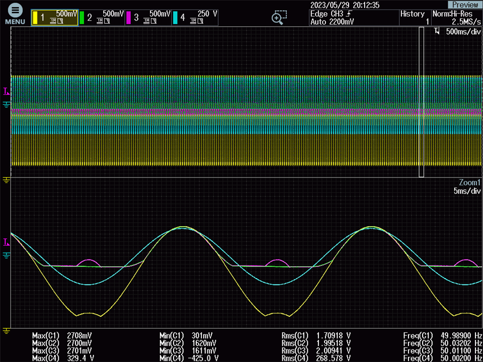
    Our LM2904's input pin(pin3/VAC_L & pin2/VAC_N) to sample one AC bus voltage. In the low temp, the output waveform of pin1 of LM2904 is clipped like below blue line. This clipping will result in AC bus voltage sampling deviation.

    What does the customer define as AC deviation?

    The waveform on the sampling resistor is sine wave like above picture.

    I'd like to know what the input signals are of VAC_N and VAC_L? 

    VAC_AD is clipped.

    Is the problem occurring at VAC_AD or VAC_DCbias_AD? 

    Currently the customer guess the clipping is related with the minimum voltage of output voltage, so they hope we can provide more detailed curve at small output current. Their output current is 0.16mA-0.2mA.

    Thanks & Best Regards,

    Sherry

  • What are the voltages at the input/output pins of the opamp when the clipping happens? The waveform looks like phase reversal, which happens only when an input voltage goes below the negative supply at pin 4. (The LM2904LV-Q1 does not have phase reversal.)

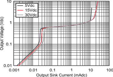
    The LM2904 (not B, not -Q1) datasheet has a better graph for low voltages; this output is slightly weaker than the B model for very small currents:

    Figure 3-2 of the Application Design Guidelines for LM324/LM358 Devices application report shows that the output is much weaker at low temperatures:

  • Hi Ladisch,

    They can't capture the waveform in the -40C low temp, so they captured the waveform at room temp as below. The channel 4 is the AC bus voltage. In order to simulate the clipping waveform at room temp, they add -50V DC bias voltage. In their real application scenario, the AC bus voltage is +/-370V.

    In their real application scenario, LM2904-Q1's minimum output is around 380mV. It seems that the minimum output voltage is larger than 380mV in low temp.

    CH1:pin1(yellow)

    CH2:pin3(green)

    CH3:pin2(purple)

    Thanks & Best Regards,

    Sherry

  • Hi Ladisch,

    It seems that the minimum output voltage is around 0.7V. But in our datasheet, we say the minimum output voltage is 20mV when adding 10kohm Rl. My customer also test this. When they add 10k, the minimum voltage is 300mV. When they add 3.33k, the minimum voltage is 223mV. But they can't get 20mV.

    Thanks & Best Regards,

    Sherry

  • The waveforms for the two input pins looks strange. In particular, their difference is much larger than elsewhere.

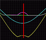
    Can you measure the voltages at pins 1/2/3 at the marked point of time?

  • Hi Ladisch,

    Thanks for your reply!

    I discussed with the customer, and they wants to know two things as below,

    1. Does our LM2904B-Q1 have below specs? If not, can we give a rough value at -40C with 0.16-0.2mA output current?

    2. During the test, they found that setting RL=3.33kohm can extend the Vo range. When they add 3.33kohm, the minimum output can be as low as 223mV while Vo_minimum=300mV with RL=10kohm. My customer wants to know whether 3.33kohm RL is ok for the application, is there any bad impact?

    Thanks & Best Regards,

    Sherry

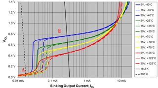
  • 1. The graph shows the typical characteristics of the LM2904-Q1. The LM2904B-Q1 has stronger outputs (the very-low-voltage region goes up to about 0.012 mA on old devices and up to about 0.05 mA on B devices).

    2. A stronger pull-down resistor increases the current that must be sourced by the output, which might limit the maximum output voltage (see figure 7-11 of the datasheet). This is probably not a problem.

    I repeat my recommendation for the low-voltage LM2904LV-Q1.

  • Hi Ladisch,

    Thanks for your reply!

    I don't understand below explanation. Could you please help clarify it? Thanks!

    the very-low-voltage region goes up to about 0.012 mA on old devices and up to about 0.05 mA on B devices

    Thanks & Best Regards,

    Sherry

  • The output has a current sink that allows very low output voltages for very low output currents; this is region "A" in the graph:

    For higher output currents, there is a full diode drop (VBE of a PNP transistor); you are seeing the temperature dependencies of that.

    Did I mention that the LM2904LV-Q1 would allow lower output voltages also for higher currents?

  • Hi Ladisch,

    Thanks for your reply!

    One more question, 

    According to above picture, the Vol is around 700mV(Vs=5V, temp=-40C, Iout=0.1mA). Currently their test value is Vol=~300mV when adding RL=10Kohm. In my understanding, it should be related with Rl load. But it is still unmatched with below spec marked in red box. Could you please help analyze it?

    In addition, the spec marked in blue box should be no significance because its test temp is 25C, right?

    Thanks & Best Regards,

    Sherry

  • The graph and the blue box are measured without a pull-down resistor.

    With a pull-down resistor, the output does not need to sink any current (or less current) to drive the actual load. In other words, this moves the output load towards or into the region "A" on the graph.

    A measured output voltage of 300 mV implies that in your circuit, the output still needs to sink more than 50 µA.