Other Parts Discussed in Thread: OPA404
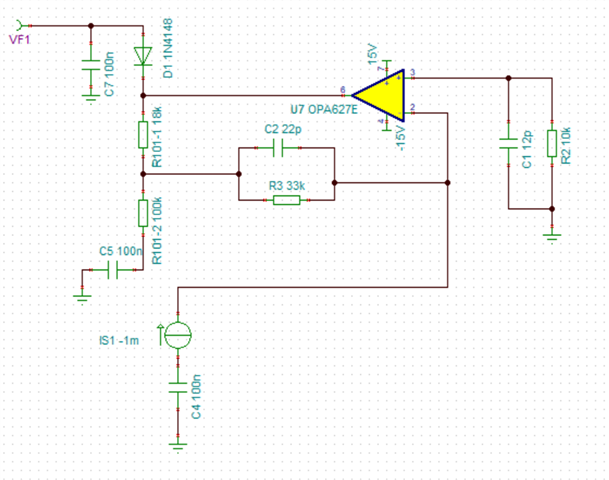
Need circuit understanding for the below opamp circuit with photodiodes (trans-impedance amplifier with T-network)
My simulation and calculation values aren't matching.
This thread has been locked.
If you have a related question, please click the "Ask a related question" button in the top right corner. The newly created question will be automatically linked to this question.
Hi Nafisa,
I have a few questions about your circuit and application.
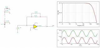
I see your feedback resistor is 33kΩ, which would indicate a gain of 33V/mA. You have included a "Tee" network to increase the gain to ~57V/mA. Why not just use a 57kΩ resistor to achieve the same gain? Achieving the desired gain without a Tee network will improve the performance of your circuit and simplify the design.
Why do you have 100nF capacitors everywhere? What are you trying to achieve with these? The 100nF capacitor at your input current source causes convergence issues with the simulator. Is this meant to represent the capacitance of your sensor input? What is your signal source?
What is the purpose of the diode at the output? Are you trying to prevent the output from going negative? If so, this doesn't work as configured...
What exactly are you trying to achieve with this circuit?
What is the desired gain?
What is the input signal current range?
What is the input signal frequency range?
What is the desired output voltage?
If you are trying to achieve a transimpedance gain of 57V/mA with a bandwidth of 220kHz the circuit shown below is appropriate.
Regards,
Zach
Hi Zach,
As this is legacy board design, we also don't have any idea on this circuit.
The output of the photodiode will be proportional to the input light, so constant light would produce a DC signal, and oscillating light would produce an oscillating signal(i.e particle detected stage). The current range of the photodiode is 0.1nA to 72mA At 780nm wavelength
Attached application image for you reference and the board design

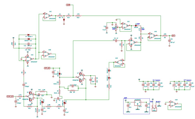
These are the voltage ranges when the particle is detected
SCAT_DC: 11.0v to 11.9v
EXT_DC: 10.3v to 10.6v
SUM: 11.0v-11.9v
EXT: 10.3v-10.9v.
Hi Nafisa,
I see this is a very interesting circuit, and very complicated as well! I'm not sure that I will be able to put all the pieces together but I will try to provide some insight. Also, the image is a bit blurry so some of the component values and voltages I am just guessing on. For now, I will limit my analysis to the OPA627 portion of the circuit.
One issue with simulating this circuit, is that placing a current source in series with a 100nF capacitor as shown in your original screenshot provides convergence issues. This is because the simulator cannot determine the DC operating point of the circuit. Seeing your wider schematic, I believe the DC operating point is set by this reference voltage and series resistor. Hard to see the exact values but my best guess is 12.1MΩ and -6V.
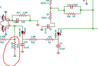
It looks like at DC the two photodiodes share the same bias current due to the AC coupling capacitors. At AC these capacitors become a short to ground and each photodiode can generate its own AC current. TINA only allows one AC signal source at a time, so I implemented the biasing circuit using a generic diode for the left circuit and a current generator with a DC bias to represent the OPA627 photodiode input.
The 18k and 2k resistors in the T-network make more sense as this increases the effective gain significantly at AC. At DC and low frequencies, the T-network is removed by the 100nF capacitor and the gain is reduced. I assume this is to provide a lower DC gain for the photodiode bias current, and a higher gain for the AC signal. This is a neat idea.
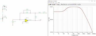
I was a bit confused by the AC coupled OPA404 loop which provides feedback to the OPA627, but I was able to simulate it.
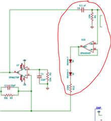
It appears that the function is to add some additional frequency shaping along with the AC coupled T-network to produce a bandpass filter effect with a center frequency of ~1kHz. This works by sensing the OPA627's output voltage and converting it into a current through the 100kΩ resistor that cancels out a portion of the current flowing through the TIA feedback network. Very interesting!
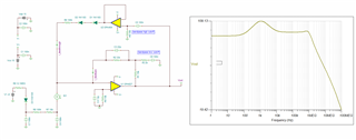
See attached TINA simulation for your reference.
I hope this was helpful. Good luck with your continued analysis.
Thanks,
Zach
Hi Zach,
Attached the profile of SUM and EXT that we got from practical testing with flow cell.
x axis time
Y axis voltage in mV
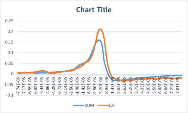
So, my question is if I want to get the similar profile in simulation as well, what sort of inputs should I provide to both SCAT_DC and EXT_DC?
Kindly help me with this.
Hi Nafisa,
From your schematic drawing, I believe these are output nodes not input nodes.
If you want to attempt to match the simulation to your real-world circuit, I would start by measuring the DC bias at various nodes of your photodiode input stage. Then you can apply the correct bias to the circuit in your simulation and see if the output nodes match up.
Regards,
Zach
Hi,
Thanks for your inputs.
I want the values for SCAT_DC and EXT_DC for the corresponding SUM and EXT profile. So for this, I am considering SCAT_DC and EXT_DC as input nodes for the SUM and EXT outputs.
For this, I have removed both the photodiodes and also the opamp U7 and U2. So, directly giving voltage inputs to the SCAT_DC and EXT_DC can give some sort of outputs, right? I am trying to get the similar profile by this method.
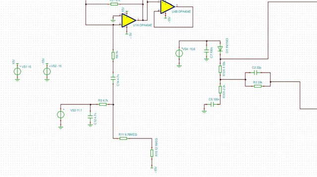
Is this the correct way to proceed? kindly confirm.
Hi Nasifa,
This approach will not work for your EXT node because you are removing the feedback component of the loop. The output is modified by itself through feedback so by removing the feedback you are fundamentally changing the output signal.
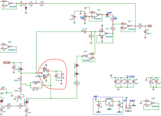
This may work for the SUM node as this node is not fed back to its input. However, you should consider that the op amp is specifically shaping the signal that goes into the SCAT_DC node and therefore it is unlikely that you can perfectly mirror this with an ideal signal source. If you were to attempt this, you should apply your signal directly where the output of the amp would be, not at the SCAT_DC node.
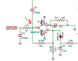
Regards,
Zach