This thread has been locked.

If you have a related question, please click the "Ask a related question" button in the top right corner. The newly created question will be automatically linked to this question.

INA234: I2C waveform Question

Part Number: INA234

Hi expert,

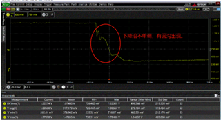
Could you please clarify if there is any risk for the I2C communication of INA234? 

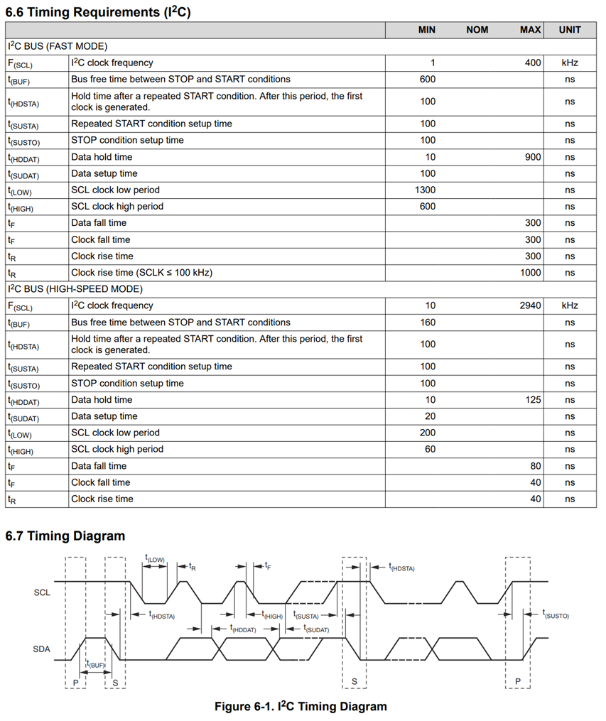
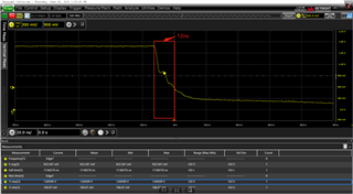
The falling edge is not smooth, and you can see up and down in below picture. 

p.s. so far I2C communication has no issues.  

Regards,

Allan

  • Hey Allan,

    I'm having a hard time seeing the time scale in your image, but you just need to make sure that your timing works with the limits in the datasheet (shown below). In general, I think it should be fine, as long as the data is in a stable location when the clock triggers. If this image if from your clock line, then there could be some concerns of accidental clock cycles, based on the variation of your pulse. 

    Regards,

    Mitch

  • Hi Export,

    I upload the legible picture, the SCL and SDA all have the non-monotonic falling edge,  its duration is about several nano-second and smallar than 15ns.

    Due to i see I2C spec requires I2C device to have a filter on both SCL and SDA input, to deal with spikes within 50ns. shown non-monotonous falling edge can be dealed with by this input filters?

  • Hi user, 

    Mitch is out of office for the holiday, so I will try and assist here. 

    Looking at the pulse, I can thnk of a few things to try here:

    - can you try reducing the pullup resistor so that additional current is allowed to flow to the lines? This might help correct some of this behavior. 

    - I do agree with your assessment that if you are seeing ringing pulses a small capacitance may be necessary on the SDA and SCL lines to smooth these out. I would place something like 1pF or something small to try and filter this HF content while not slowing the line down much

    - I spoke with some of our validation team about this issue and they also commented that the address lines can sometimes have an effect on communication. If the pins for addressing are connected to Vs or GND, placing capacitors on the address lines close to the device will also potentially provide benefit here. 

    Please try the above and let us know if any of these help alleviate the issue. 

  • Hi export,

    I tried to add small capacitance and change the pullup resistor, the SCL and SDA falling edge can be improved, but it still have a step, could you help to check if the step is ok? Many thanks!

  • Yes, this looks better and I think it will be fine.