This thread has been locked.

If you have a related question, please click the "Ask a related question" button in the top right corner. The newly created question will be automatically linked to this question.

OPA855: oscillate in output

Part Number: OPA855

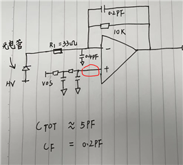
Our Customer Use OPA855 in a TIA circuit. Following is their test environment, right side for TIA is oscilloscope and the other is a photodiode.
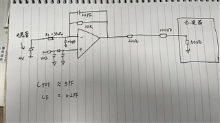
But there is a high frequency oscillation. Following is waveform, yellow is TIA output, pink is FFT frequency domain waveform. As the waveform shows, There is a 3.3GHz noise with a 100Mhz envelope signal. Customer changes the capacitance, but there is no effect.
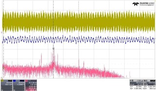
What should they do to reduce the noise? Hope you could give they some method to avoid this.

  • Hi Minghao,

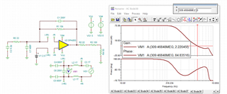
    After looking a stability analysis of the circuit, you shared, it appears the circuit is stable. I did make some assumptions based off the values you provided, but overall, the representation of the circuit I simulated seems stable. The circuit is attached below.

    4454.OPA855_stability.TSC

    With this information I did have a few questions.

    Is there a PCB layout available for this circuit? The reason being that additional parasitics can be introduced depending on the layout of the board.  This could cause the circuit to become unstable. 

    Is there a reason for the 33-ohm resistor? Is this modeling the photodiode? This could cause some confusion in the current to voltage conversion and result in unexpected results.

    I would also like to point out that the circuit with the current load is not matched to the oscilloscope, which could result in unexpected results due to this mismatch. We recommend matching to the instrument's input impedance to limit any reflections that might occur.

    Best Regards,

    Ignacio

  • I talk with customer about this problem. We think this problam may caused by phase margin is not enough. For 3.5GHz signal, the phase delay is 180 degree, and the TIA circuit bring another 180 degree delay. Is it a reason cause that?

  • Hi Minghao,

    You are correct, when an op amp circuit is oscillating the phase margin of the circuit is not adequate. In this oscillating state, the circuit is unstable and oscillates at a somewhat unpredictable frequency which is likely what is being seen with the signal at 3.5GHz. The circuit configuration is what causes this phase shift to occur between the signals at the two inputs and if enough phase difference is present, this is when the circuit becomes unstable leading to oscillations. However, from the analysis I shared previously, the circuit does seem stable using the component values that were shared. 

    The design of the PCB also affects the phase margin of the circuit due to unwanted parasitics, which maybe be a reason for the stability problems occurring. Although not as common, we have also seen oscillations due to improper voltage supply filtering. The combination of poor filtering of the supplies with less-than-ideal PCB layout has resulted in oscillation type behavior at the output of the amplifier.

    Best Regards,

    Ignacio

  • Hi Minghao,

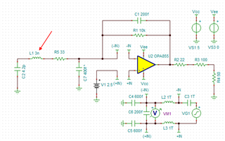
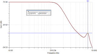
    The team was able to look more into the phenomenon you were seeing at the higher frequency, and we are inclined to believe that it is likely due to non-ideal characteristics of the photodiode. By assuming non-ideal characteristics such as bond wire inductance, which can be roughly estimated we were able to see a peak around the 3.3GHz originally measured.

    This non-ideality can be modeled as an inductor in series with the capacitance of the diode like the image below shows. Running the stability simulation shows peaking in the range you were measuring. The theory is that the extra inductance is isolating the diode capacitance and is noise-gain shaping at the higher frequencies. 

      2642.OPA855_stability.TSC

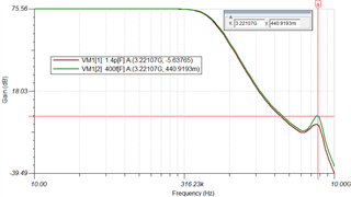
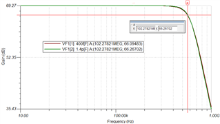
    A suggestion to counter this is by adding more capacitance at the inverting node to ground. Below is a simulation that simulates the circuit with the original input capacitance of 400fF (green trace) and one with the added capacitance of 1.4pF (maroon trace). The results show less peaking at those higher frequencies.

    We also ran a closed loop bandwidth simulation and the results showed that the added capacitance should not affect the system's bandwidth.

     OPA855_BW.TSC

    As was mentioned previously non-idealities in the APD seem like a cause for this issue you are experiencing but similar non-ideal parasitics also arise from PCB layouts not applying best practices. 

    Best Regards,

    Ignacio

  •  Hi, the datasheet shows when the state changes there will be an oscillate. And It seems is a 100MHz signal. Is this right? Is there is any way could reduce or inhabit the oscillate? The frequency is fix 100MHz?
  • Hi Minghao,

    The datasheet graph you are referring to is highlighting the turn-on/turn-off delay when you power the device on or off. The signal expected at the output is the 2Vpp signal, and the delay of 15ns in the graph highlights the 15ns delay in the Electrical Characteristics table under Power Down.

    Best Regards,

    Ignacio

  • Customer found their circuit phase margin is very small about 10 degree. But because of PCB layout, they can't change the circuit, I suggest they change the bandwidth, but they also can't change it. Is there any method to help them?

    customer also want to know for what the close-loop output impedance change for high frequency, still increase?

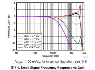
    And for this part, is this a zero point front 5GHz? Why it looks so smooth in 7V/V? But it's different for -7V/V? 

  • Hi Minghao,

    Is there a way to add extra input capacitance to the circuit board just to test if this helps their oscillation problem, this will narrow down that the PCB layout is likely causing some instability.  Could you also provide the analysis they did to get the phase margin they are getting?

    As for the closed loop output impedance question, I can look further and see if there is any additional data at higher frequencies as closed loop output impedance depends on a couple factors. 

    The reason you are seeing a difference between +7V/V and -7V/V is because the amplifier is configured is in a different configuration. Although they are both in a signal gain magnitude of 7V/V, the noise gain for the two configurations is different. This configuration difference is what results in the performance variation seen in the datasheet despite both being in a signal gain magnitude of 7V/V.

    Best Regards,

    Ignacio

  • Hi Minghao,

    I was able to ask for information on the closed loop output impedance and we can assume the output impedance should maintain the slope shown on the datasheet plot up till about 6GHz.

    Best Regards,

    Ignacio

  • If customer has a large input capacitance but they don't want to reduce bandwith, Is there any recommended TIA circuit?

  • You are probably seeing an input transistor self oscillation due to those caps looking out the V+ input, try putting a 10ohm R here, Or at least try removing that last cap looking out the V+ input and changing that last R to 10ohms