This thread has been locked.

If you have a related question, please click the "Ask a related question" button in the top right corner. The newly created question will be automatically linked to this question.

INA190: Problem with current measure on a high voltage line

Part Number: INA190

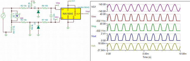
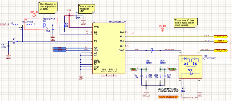
I am an electronics engineer at Laclarée, a French startup, designing electronic eyeglasses for presbyopia correction. In our eyeglasses, we have a MAX14521E for generating a +/- 140V square wave signal needed to the deform the membrane of our lenses. This signal can be considered to be connected to a capacitive load ranging from 0 to 8 nF. We would like to measure the current consumption of this capacitive load connected across OUT_A- OUT_COM or OUT_B- OUT_COM.

HV driver

INA190A1 circuit

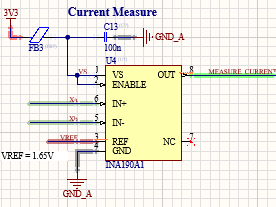
Our measurement and feedback section is placed on the COM line as shown in the figure above. We want to use the INA190 due to its low power consumption. Even though the current measure section is after the load, the voltage on the COM line is still +/- 140V. This complicates the direct measurement of current using the INA190. The output signal of the INA190 is expected to be in the range of 0-3.3V and capable of measuring 0-8mA. I have implemented a voltage divider to reduce the common mode voltage but it is not clear to me if this is the right implementation. Could you kindly help me with this?

  • Hello Valued Engineer,

    I am looking this over and will respond shortly.

    Sincerely,

    Peter

  • Hello

    Using the INA190 with resistor dividers at the input pins is not usually recommended. First, you would need to half-wave or full-wave rectify the Vcm because the minimum Vcm for the device is -0.3V.

    Second is that you will need very accurate (low-tolerance) resistors to create tight matching between inputs in order to reduce input bias offset error. This will increase cost and create tradeoff between circuit accuracy and power loss from leakage.

    If you do go this route with input resistor dividers, you will want to insert a large input differential capacitor (>1nF) in between IN+ and IN- pins. This requirement is specific to the INA190 because it helps keep the input switching stage stable when loading the input pins with resistance. This requirement will mean you will lose BW.

    Lastly, input resistance will affect the device gain error as per datasheet equation:

    One last note about using the INA190 (or any other current sense amplifier with a -0.3V minimum Vcm) is that you may want to consider only measuring the half-wave rectified current by placings diodes to ground off INA190 inputs. These diodes should ideally clamp the input Vcm to -0.3V. Here is an example below. Note I use R6 and R7 to limit input current into device pins because the clamping diodes D1 and D2 will not ideally have a Vf of 300mV, but it could be higher and thus you will need to limit the turn-on current of internal ESD diodes to less than 5mA (I would not exceed 2mA for margin).

    If you must measure both positive and negative peaks, then you could use two amplifiers. However, in order to measure the current for -140V, you will need to full-wave rectify the voltage. But this adds more complexity because this full-wave rectifier creates a separate load current in parallel to the 8mA load. So to measure the true load you would have to measuring the current divider between these two currents.

    Sincerely,

    Peter

  • Thank you for the response Peter. Since we are operating on an high voltage line, the voltage divider seems inevitable. We will make the output signal of the MAX14521E only positive, i.e. 0-140V. This should eliminate the need for the rectification section. Do you recommend any other amplifier configuration that can reduce the complexity of this measurement? The main constraint we have is that the current consumption of the amplifier (ideally <200 uA). 

    Sincerely,

    Devaraj

  • Hello Devaraj,

    My apology for the delay.

    Well if this is the case, then you can use the same circuit I provided in last post, but without the clamping diodes D1 and D2.

    You will have to fine tune the resistors here to account for power leakage.

    Also what is the frequency of this signal? You will want the effective differential cutoff frequency of the input filter (fc_diff) to be greater than signal frequency so you don't attenuate peak signal. fc_diff = 1/(2*PI*Rf*2*Cdiff) where Rf = R3||R4 and Cdiff = C1 according to the simulation schematic I sent in last post. Like I said you will definitely want Cdiff to be >= 1nF to keep input signal stable given that you are going to load down input pins with the resistor dividers. 

    If bus frequency is high compared to INA190 BW or you need low distortion at low currents, then you may want to consider adding a bias/reference voltage (~100mV) at INA190 REF pin so that OUT is not saturating when Vbus = 0V. This will prevent any overload recovery distortion and delays. You also can negate any offset error by measuring the differential output voltage. Refer to this application note for more information:

    https://www.ti.com.cn/cn/lit/an/sboa551/sboa551.pdf 

    Sincerely,

    Peter