This thread has been locked.

If you have a related question, please click the "Ask a related question" button in the top right corner. The newly created question will be automatically linked to this question.

INA333: INA333 output is not amplified and is odd on an oscilloscope for an EOG circuit

Part Number: INA333
Other Parts Discussed in Thread: OPA2333, INA826, OPA392
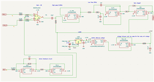
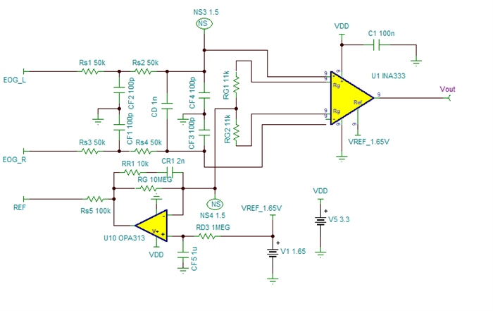
The circuit is shown above

Application : I'm using the INA333 amplifier as my first gain stage that takes two inputs from horizontal EOG electrodes placed on the sides of the eye close to the temple. I take the common mode at the middle of two matched gain resistors, invert it and biased against the stable 1.65V reference to feed it into the body through the reference electrode. I expect to see an amplified output by a factor of 20. But none of that happens. If I hook up the output to the oscilloscope, it's weird, just a ton of noise and small amplitudes. When I used a voltmeter, the inputs were around .7-.8mv and the output was between .7-.8mV. NO Change to the outputs. While common mode was around .175 mv. I also thought the voltage at the reference would be around 1.65 as it's biased to that voltage but it's ~ .8mV just like the inputs. 

The circuit was hand soldered on a perfboard. Also one thing the circuit does not include which the soldered board includes is a decoupling capacitor of 0.1uF between the positive rail 3.3V and ground for all the opamps.
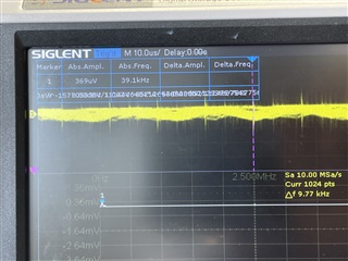
That's the oscilloscope output, the top is the signal and the white graph below is the fft. The table contains markers of the peaks, in this case just one peak and at some KHz?!

Based on my understanding of the datasheet of INA333 and opamps in generally, I feel like I've covered all the bases. I don't quite understand why my output is not amplified. The only other thing I can think of doing is ordering a layed out PCB.

Anyone have any possible solutions of experiments to potentially work through to solve this problem. 

  • Hi Roshan,

    There are a few comments/suggestions the circuit:

    - Please add low-pass filters at the INA333 input with a low frequency corner to filter all the extrinsic high-frequency noise.  The EOG signal of interest is relatively low-frequency.  The differential capacitors of the low-pass filter will also help minimize the effects of the high-source impedance with the chopper instrumentation amplifier input bias (IB) current spikes. 

    - The EOG signal is an AC +/- differential signal, therefore, the INA333 REF pin needs to be biased at Vs/2 = +1.65V to amplify the signal properly. Connecting VREF=GND will not work.

    - The integrator of the feedback REF circuit needs to be referred to a reference set to mid supply or +1.65V.  See a similar integrator example below. You may need to adjust the circuit depending on your probe impedances and requirements.


    Below is a link for reference design for an ECG application using the OPA2333 in a difference amplifier + ADC circuit.  I realize that your circuit is for an EOG application, and the reference design is for a different ECG application.  Nevertheless, please review this document in detail, as many of the concepts are quite similar. 

    https://www.ti.com/lit/ug/slau516/slau516.pdf

    https://www.ti.com/tool/TIPD116

    Please let us know if you need anything,

    Thank you and Regards,

    Luis Chioye

  • Hi Luis,

    Thanks for the detailed response, a few questions based on your explanations:

    - It was always my understanding that the EOG was a DC signal, but it is made AC to remove the dc offsets, do you mind clarifying? Or do you mean that since I'm already AC coupling the circuit, that we treat EOG as an AC signal. So, would the other way to approach if I were to treat it as a DC signal not require any high pass after the first gain stage and just a high precision ADC?

    - I understand the need of a low pass filter at input for the intrinsic noise, in that case I assume there is no need for a low pass after the first gain stage right? But it is also my understanding that placing any components in front of INA333 might result in an increase in offset voltage. Where IB current spikes coming from closing/opening of the front-end switches is converted across the mismatched input impedance into voltage causing an increase in the offset voltage. Hence doesn't it seem like adding an EMI (LPF) filter at the output of INA333 the better approach. But that brings me back to where I'm at with this weird output, only making sense to try something different.

    - "The integrator of the feedback REF circuit needs to be referred to a reference set to mid supply or +1.65V" - I actually did that in my attached circuit, unless the one you shared is fundamentally different. Do you mind giving me some advice as to what to change based on electrode impedance measurements

    - INA333 REF pin needs to be biased at Vs/2 = +1.65V to amplify the signal properly -> why can't it be biased after the amplification?

    Sincerely,
    Roshan

  • HI Roshan,

    It was always my understanding that the EOG was a DC signal, but it is made AC to remove the dc offsets, do you mind clarifying? Or do you mean that since I'm already AC coupling the circuit, that we treat EOG as an AC signal. So, would the other way to approach if I were to treat it as a DC signal not require any high pass after the first gain stage and just a high precision ADC

    The EOG signal is a low-frequency signal. Most literature describe the EOG electrode signal in the low frequency range is DC 0-Hz to 50-Hz, or other articles define it in the range of ~0.1Hz to ~20Hz. The signal is relatively small in amplitude in the 100s of microvolt to millivolt range. Since the signal of interest is a small-amplitude, low-frequency signal, the user needs to eliminate any external EMI and high-frequency noise interference from the environment.  Using low-pass filters at the instrumentation amplifiers such as the INA333 is standard practice, as shown in the proven design listed on the application note.  

    - I understand the need of a low pass filter at input for the intrinsic noise, in that case I assume there is no need for a low pass after the first gain stage right? But it is also my understanding that placing any components in front of INA333 might result in an increase in offset voltage. Where IB current spikes coming from closing/opening of the front-end switches is converted across the mismatched input impedance into voltage causing an increase in the offset voltage. Hence doesn't it seem like adding an EMI (LPF) filter at the output of INA333 the better approach. But that brings me back to where I'm at with this weird output, only making sense to try something different

    The low-pass filter at the instrumentation amplifier input is used to eliminate external or extrinsic noise, but not the intrinsic noise of the circuit. 

    The original post circuit uses only resistors with no capacitors, which will not work. The high-impedance resistors will amplify the IB current spikes of the chopper amplifier and increase noise.  In contrast, the example provided on the reference design uses the high-impedance resistors with a differential and common-mode capacitors, creating a low-pass filter. 

    The filter uses a differential 1nF capacitor across the instrumentation amplifier inputs and 100pF common-mode capacitors.  These capacitors at the INA333 inputs offer a low equivalent impedance at the instrumentation amplifier inputs, or a relative low-impedance path at the chopper frequency, and therefore, the capacitors help mitigate the effects of the chopper IB current spikes.  Also, the low-pass filter help reducing EMI noise at the inputs of the instrumentation amplifier, which is absolutely required, specially when attempting to amplify small low-frequency signals.

    "The integrator of the feedback REF circuit needs to be referred to a reference set to mid supply or +1.65V" - I actually did that in my attached circuit, unless the one you shared is fundamentally different. Do you mind giving me some advice as to what to change based on electrode impedance measurements

    Yes, I see that you referred the integrator to +1.65V.  The impedance of the electrodes is dependent on the electrode/probe type. If you provide the electrode impedance model, then we could check the integrator for stability.   

    - INA333 REF pin needs to be biased at Vs/2 = +1.65V to amplify the signal properly -> why can't it be biased after the amplification?

     Keep in mind that the amplifier output can only swing within the supply rails and requires a minimum ~50 millivolt headroom above or below the rail supplies, where the INA333 is powered with uni-polar supply of +3.3V and GND. The minimum output of the INA333 in this circuit is around +50mV.  Therefore, when using REF = GND on the INA333, this setup limits the output swing to only positive input signals, and limits the output range of the INA333.  This becomes an issue for small differential signals.  Also, the INA is required to amplify the voltage difference on the electrodes, which in most applications, the difference on the electrodes can be positive or negative voltage.

    Thank you and Regards,

    Luis

  • In this link, https://www.ti.com/video/6269751746001?context=1148465-1148591 they rather recommend a buffer at input, is this because of the differences in ina333 and ina826?

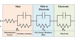
    I'm using dry electrodes, so something like this is the equivalent impedance model, can you please inform me of the stability:

    Best,

    Roshan

  • Hi Roshan,

    Dry electrodes may require higher input impedance, and in some instances, certain dry electrodes may not be able to drive a chopper amplifier. Non-chopper, CMOS or JFET input amplifiers such as the OPA392 can be used as buffers for these applications. These CMOS amplifier exhibit typical input bias currents well below ~10pA. Although the INA333 is a chopper, it still offers relatively low average input bias current amounting to ~70pA typical (200pA max). Nevertheless, if your specific electrodes require a very high-input impedance, you can certainly buffer them using a CMOS input amplifier such as the OPA392. 

    The actual impedance (R, C) values on the electrode model above are required for the stability analysis. The impedances on the model are specific to the electrode on the application and need to be defined on your side.

    Thank you and Regards,

    Luis 

  • Would it make a difference to place the buffers before or after the input filters?

    I am modelling a range of electrode impedances based on material and pressure that I will be dealing with, i'll drop in a reply when I get that.

  • HI Roshan,

    Please place the buffers after the low pass filters, at the inputs of the INA333.

    Thank you and Kind Regards,

    Luis