This thread has been locked.

If you have a related question, please click the "Ask a related question" button in the top right corner. The newly created question will be automatically linked to this question.

TLV9064: Amplifiers forum

Part Number: TLV9064

Hi team,

My customer has been using TLV9064 for many years, but the latest batch of TLV9064 seems to have a larger Vos value than before, the codes are 32AG3P0Q0 and 32AG3P0XC.

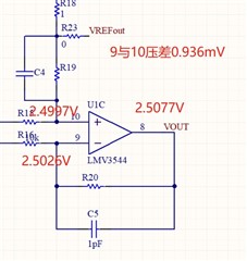
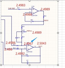
Here are the actual results of the customer's testing. When they do not account for the loss, Vos = 2.4989 - 2.4967 = 0.0022V.

This situation is an occasional issue and the Vos is usually ideal when the customer changes to a new TLV9064 device.  

Could you please give some comments for the issue? Thanks in advance!

Regards,

Ivy

  • Hi Ivy,

    Thanks for sharing the customer question and schematic.

    A 2.2mV  input offset voltage should not exist on TLV9064 as the max room temperature offset is +-1.6mV and max over temp is +-2.0mV

    Can the customer share the component values for R20, R19, R15, C5 and C4?

    Generally speaking parts do age and experience shift  in specifications, but this is generally something that takes a significant amount of time to be measurable. 

    If the customer can verify these values, we can have a better idea of what may be causing this response,

    Thank you,

    Jacob

  • R19和R20  49.9KΩ,0.1%

    R15和R16  10KΩ,0.1%

    C4和C5: 1pF

  • Hello Ivy,

    These values make sense, I understand the application.

    What is the percentage of devices are exuding this behavior?

    How long is the old part on the board to see this high Vos?

    How is the customer measuring these voltages? I just want to make sure the system is in steady state when the voltage reading is occurring.

    Thank you,

    Jacob

  • 1, defective rate 0.5%;
    2, after assembly through 5 high and low temperature cycles (no electricity), each cycle of 125℃ 30min-->-40℃ 30min;
    3. Data measured by a multimeter

  • Hello,

    Thank you for the additional details on the testing. We are going to conduct a series of internal rests to evaluate if this behavior can be observed on our end.

    Temp cycling the device effectively stresses the silicon and the mold compound, consequently shifting parameters like input offset voltage. We characterize behavior like this in our temp cycle tests, however all of these tests are completed with power to the device. The Datasheet accounts for shift in parameters caused by temperature changes, so I am still working to understand what could be causing this issue.

    What is the resolution of the multimeter used? 

    Thank you,

    Jacob

  • After we do not charge -40~125 for 5 cycles, there will be -40, 0, 25, 65, 85, 105℃ offset temperature drift test (at this time is powered on), each temperature point stays for about 10 minutes

    The multimeter uses 5 and a half bits

  • Thank you for the additional information.

    Some additional Vos can be introduced by stressing the package. Have you tried to de-solder a high Vos part and then re-solder it back on the board and measure Vos?

    Sometimes the different coefficient of thermal expansion values between the PCB and package can cause extreme stresses which shift parameters of the device.

    Can you try this test with a high Vos device? I would be very interested to see if this alters the Vos value. 

    What is the power supply voltage for the part? This will tell me what region you are in for the input stage transistors.

    Thank you,

    Jacob

  • NG chip welding back to the original position, tried, the output is still beyond (-5mV~5mV) range;
    The chip power supply is 5V;

  • Hello Bao,

    I appreciate your patience as we debug this case.

    Thank you for the additional details, this helps me confirm the region the input stage is in.

    When you say "output is still beyond (-5mv ~5mv)" is this accounting for the gain of the amplifier?

    Can I see the voltages at nodes (8, 9,10) to ground from your most recent testing? Also, can you probe between pins 9 and 10 with the DMM? I want to make sure GND shift is not a factor in the Vos reading.

    We are currently running tests on our end to see if we can replicate any behavior like this. This is not something we have seen before.

    Thank you,

    Jacob

  • The pressure difference between pin 9 and pin 10 is 0.936mv, and the rest is shown in the figure

  • Hi Bao,

    Thank you for the measurement, This part is behaving as expected. Vos: 936uV

    Do you have any parts which exude greater than 2mV Vos between the inputs when measured like you have done here?

    Our tests so far have not been able to replicate the numbers you had reported in the previous pictures in this thread.

    Best,

    Jacob