This thread has been locked.

If you have a related question, please click the "Ask a related question" button in the top right corner. The newly created question will be automatically linked to this question.

OPA858: How to Place the AC-coupling capacitance and resistance in a TIA circuit in PCB layout

Part Number: OPA858

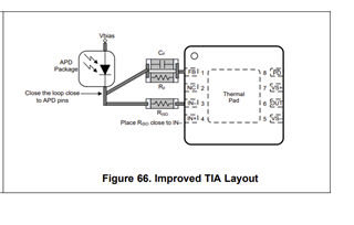
I am planning to use OPA858 as the Transimpedance Amplifier for the following TIA circuit. C2, R8 are to AC couple the circuit: 

In the data sheet of OPA858, it recommends using this layout with Riso in order to reduce the resonance between the trace and the Transimpedance amplifier's internal capacitance. My question is with my R8 and C2, where should I close the feedback loop and where should I put my R8 and C2? In our application, we cannot put the C2 very close to the PD due to physical limitations. Our bandwidth of interest is 1-30 Mhz. 

  • Hi Tong,

    The feedback loop is always closed to the -IN pin, however when using a Riso resistor you close the loop on the other side of the Riso (R11) like you have in the schematic. With the addition of R8 and C2 you would have to fit in the two components as close as possible, however they will be connected how the schematic is shown. I would like to mention that there is an added complexity and set of drawbacks to AC coupling the signal, did the circuit provide the expected results when simulating? If so, please disregard my comment.

    Best Regards,

    Ignacio

  • Thank you so much! The simulation results are correct. Do you mean that the R8 and C2 needs to be as close to the input pin of the TIA as possible? But the data sheet said I need to close the loop close to the photodiode? 

    Also, I wonder the necessity of Riso, our signal frequency is 1-30 MHz and 50uA. 

  • Hi Tong,

    At these frequencies Riso will likely cause more harm than good so you should have no issue removing the resistor. With this resistor gone, the feedback components should connect straight to the -IN pin and all your other components should be as close as possible to the -IN as well. Making the design is as close as possible including the PD will limit any parasitics. The board will be connected the same as the schematic, however in terms of layout ensure it is all as close as possible to the -IN pin and that your feedback trace to your -IN pin from the feedback components is as short as possible like Figure 65 highlights.

    Best Regards,

    Ignacio