This thread has been locked.

If you have a related question, please click the "Ask a related question" button in the top right corner. The newly created question will be automatically linked to this question.

TLV9062: Cost optimized design for 4-20mA current loop measurement & CT measurement

Other Parts Discussed in Thread: TLV9062, TLV9002, TLV07, INA351, INA199, INA181, TLV333

Hello Community,

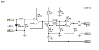
We are working on a highly cost-sensitive Data Acquisition system and seeking your valuable expertise to guide me through the design process. The system involves measuring the voltage drop across a Shunt resistor, which is connected in series to the signal circuit loop. The signal circuit loop can either be a 4-20mA current loop or the secondary side of a Current Transformer (CT).

Measuring Circuit Details:
- Supply Voltage: 0 to 3.3V
- ADC Input Range: 12-bit unipolar, 0-3.3V (adjustable to 2.048V, 2.5V, and 2.9V)
- Expected Bandwidth: Up to 2/3kHz maximum
- Separate grounds for measuring circuit and current loop circuit

Current Loop Circuit Details:
- Supply Voltage: 0 to 36V
- Current signal in the loop 4-20mA

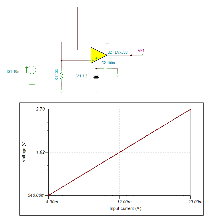
Secondary Side CT Details:
- The CT has a turn ratio of 1:2500
- Shunt Resistor (Burden resistor) can range from 5 Ohm to 50 Ohm (lower the better)
- Ability to adjust shunt resistor value for burden resistor on the secondary side of the CT to match ADC dynamic range based on the current being measured (adjustability is preferred)

I am relatively new to Analog circuits, and my team and I are facing challenges in converting analog signals into the digital domain with the required accuracy & confidence. We are looking for your guidance to navigate this design process efficiently.

The system will be utilized to measure fairly slow-moving physical quantities like Temperature, Pressure, etc., via the 4-20mA current loop. Additionally, we will also be measuring current with a lower shunt resistor across a Current transformer.

  • Acceptable Error: 0.2-0.4% max
  • Using low-cost MCU with 5 built-in 12-bit ADCs (hardware oversampling) for improved SNR.
  • Measuring slow-moving physical quantities like Temperature, pressure etc via a 4-20mA loop.
  • Measuring current consumption with a smaller shunt resistor across the Current transformer's secondary side.
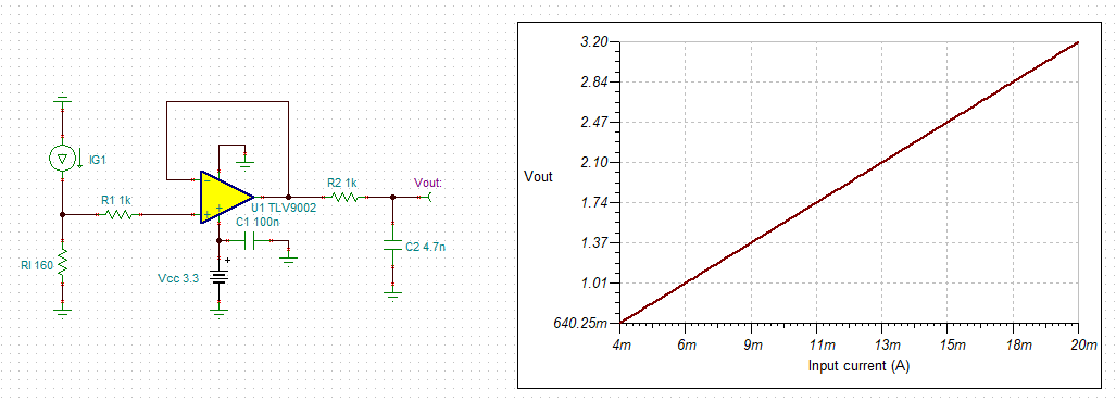
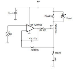
  • OpAmp Shortlisted: TLV9062, TLV9002, TLV07,
  • Current Sense Amp Shortlisted: INA351, INA181, INA199.
  • Seeking circuit design suggestions: minimal discrete components, cost-optimized & highly integrated solutions.

Thank you in advance for your support and valuable input.

  • Hi Shreeneet, 

    Thanks for providing a lot of information about the system and required specs. Do you have any basic block diagram of what you are envisioning the circuit will look like? 

    Best Regards, 

    Robert Clifton 

  • Hello Robert,

    We have explored several reference designs, but the presence of numerous discrete components in the circuits is not ideal for our requirements.

    We received valuable guidance from @Art & @Raymond from the Precision OpAmp team, suggesting a solution. However, the cost of the  TLV333 OpAmp exceeds our budget for this particular use case.

    As a result, we are considering using TLV9002 or TLV9062, but before finalizing the design, we would greatly appreciate feedback from the TI Community on these decisions.

    Specifically, we seek input on the following points:

    • How can we minimize errors in the unity gain configuration with a Voffset of 1.6mV?
      • Which Offset value should we consider, the typical (0,4mV) or the maximum (1.6mV) value as per the datasheet?
    • How can we reduce the need for external components in the CT's secondary side measurement, where a gain up to 50 may be required without exceeding the error budget of 0.2-0.4%?
      • INA351 & INA181 appear to fit our budget requirements well
      • What shall be the impact of the relatively higher Voffset in these Current Sense amplifiers on the FSR error?
      • How do we minimize these errors with better design decisions?
    • Are there any additional filter, ESD, surge, and overvoltage protection measures we should consider without compromising the signal chain characteristics?

    As we are relatively new to Analog circuits, any guidance and insights from the community would be immensely helpful for me and my team.

    Thank you for your time and support.

    Best regards

  • Hi Shreeneet,

    How can we minimize errors in the unity gain configuration with a Voffset of 1.6mV?

    You have several options. One option is doing a one time calibration to check what the offset error is then use the onboard software or hardware to adjust for this. I believe Art did mention this in that previous thread.

    The second option, use a different op amp with lower offset voltage and accepting the higher costs for a more precise device. 

    Which Offset value should we consider, the typical (0,4mV) or the maximum (1.6mV) value as per the datasheet?

    Both. Typical will be for what you typically expect to see, and the maximum will be designing for the worst case error. If you have a way to calibrate it the system that would greatly help minimize the effects of the offset. 

    How can we reduce the need for external components in the CT's secondary side measurement, where a gain up to 50 may be required without exceeding the error budget of 0.2-0.4%?
    • INA351 & INA181 appear to fit our budget requirements well

    Using the INA351 or INA181 would help reduce the external components since they have the gain resistors integrated.

    To be honest, you are reaching the point in your design where you need to decide whether you want to go with a more integrated solution or discrete solution.

    What shall be the impact of the relatively higher Voffset in these Current Sense amplifiers on the FSR error?

    A relatively higher offset means there will be relatively higher error in the signal. 

    How do we minimize these errors with better design decisions?

    Answer is the same as the first question's reply. 

    Are there any additional filter, ESD, surge, and overvoltage protection measures we should consider without compromising the signal chain characteristics?

    Op amps have internal ESD protection on both the inputs and outputs. TVS didoes on the supply rail pins can help with overvoltage protection. 

    Best Regards,

    Robert Clifton 

  • Hello Robert,

    In the following circuit, the Shunt Resistor is connected to the ground of the measuring circuit. The measuring circuit is operating at 0-3.3V while the Current loop circuit is operating at 0-36V. Can you confirm if we can continue with the following suggested design or do we need to make any updates in the following design?

    A relatively higher offset means there will be relatively higher error in the signal. 

    I meant to ask does this error gets multiplied by the Gain in the configuration.

    To be honest, you are reaching the point in your design where you need to decide whether you want to go with a more integrated solution or discrete solution.

    We are looking for an integrated solution for CT-based Current measurement via Burden Resistor with gain of 5 to 50, this is clear to us. We seek guidance to help us locate better components as we have limited exposure to the TI portfolio. Once you understand our requirements, you might be able to help us with better component suggestions.

    We are looking for a robust solution with a relatively relaxed error budget of up to 0.4% for both applications, looking forward for your valuable insights on which components may help us achieve a better fit between integrated solutions as well as lower costs as we have limited exposure to the TI portfolio.

  • You have several options

    Can you share these options with us? Also for one-time calibration of the offset, we have a unipolar ADC, will this cause any calibration constraints?

  • Hi Shreeneet, 

    Can you confirm if we can continue with the following suggested design or do we need to make any updates in the following design?

    This is a pretty simple circuit. It looks like it should be ok based on the information you have decided. Only you can decide whether or not you should move forward with a design. 

    A relatively higher offset means there will be relatively higher error in the signal. 

    I meant to ask does this error gets multiplied by the Gain in the configuration.

    I'm sorry I misunderstood. Yes the error will get multiplied by the gain. 

    Can you share these options with us? Also for one-time calibration of the offset, we have a unipolar ADC, will this cause any calibration constraints?

    I would recommend asking the ADC team this question. Which part number is this? Please create a new post asking to better understand any limitations and how to use it. 

    Using the ADC is one option. Another is using a DAC. But if you don't have a DAC then I would recommend sticking with the ADC calibration method. 

    Best Regards, 

    Robert Clifton 

  • Hi Shreeneet,

    Current Loop Circuit Details:
    - Supply Voltage: 0 to 36V
    - Current signal in the loop 4-20mA

    Here is an example of low cost discrete 4-20mA current loop transmitter. The accuracy or errors depends on the quality of the components you used in the design. 

    TLV07 Discrete 0-3.3V 4-20mA 07252023.TSC

    Alternatively, you may use V/I converter, and it may work as well. Regardless what you are selecting, you will need an ultra stable LDO or bandgap reference for the discrete 4-20mA V-I converters, since temperature change and drift of digital data recorder is critical to the application. 

    https://www.ti.com/lit/an/sboa327a/sboa327a.pdf?ts=1690316800099&ref_url=https%253A%252F%252Fwww.google.com%252F

    Best,

    Raymond