This thread has been locked.

If you have a related question, please click the "Ask a related question" button in the top right corner. The newly created question will be automatically linked to this question.

XTR111: XTR111 current varries with load resistor.

Part Number: XTR111

Hello Team,
This thread is a continuation of my previous post Link.

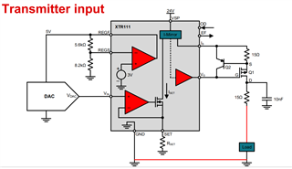
We are using XTR111 in one of our projects.
Attached is the schematic for the same.


We need both analog voltage (0 to 10V) and analog current (4 to 20mA) outputs.
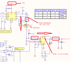
So we are using a mux to switch between voltage and current.
A DAC is used to provide voltage at the VIN pin of the XTR111.
The resistor Reset is 2.5K
So the voltage input at the VIN pin corresponding to 20mA is 5V.
But we are getting only 18V when 5V is applied at the VIN pin also, the current seems to be carrying with the load.
When we connected a 500E resistor, the current was 18mA and it suddenly dropped to 16mA when the load resistance is increased to 1K resistor.
What could be the reason for this? 

Analog Output1.pdf

  • Hi Shibin,

    In the XTR111 schematic above, multiplexer and circuitry are powered with bipolar ±15V supplies. The XTR111 is powered with +15V supply.

    The XTR111 is a 3-wire current transmitter, the general recommendation is to refer the load resistance to the same GND potential of the current transmitter as shown below. Under the recommended circuit, a 20mA current through 1kOhm resistor, will produce 20V,  which is not possible.

    The XTR111 requires a minimum compliance of at least +(VVSP-2V) at the IS pin.  Since the device is powered by a +15V supply, the maximum voltage at the XTR111 IS pin needs to be less than +13V.  In the circuit, the designer must also allow headroom for the external PFET transistor VSD voltage, around ~0.2V-0.3V, and the voltage drop due to the total series resistance in the current path.  In your schematic, the circuit has additional series resistance of R229, R234, R235, and the internal mux RON (~4.5-Ohm max) resistance.

    In short, the XTR111 device can only provide a 20mA current to a load resistor below < ~590Ω while powered with a +15V supply and when accounting for the required XTR111 2V supply compliance, and all the VDS and series resistance voltage drops involved.  See below:

    Please refer to the TI Precision Labs tutorials on the links below:

    Current loop transmitters: Analog input 3-wire 4-20-mA transmitters

    Thank you and Regards,

    Luis

  • Hello Luis,
    Thank you for your reply.
    The P Channel MOSFET we are using is SSM3J356R,LF.
    Can you please comment on this selection?
    Can you please explain the total current consumed from the 15V rail by the XTR111 when it delivers a 20mA output current?
    In our case, the maximum load resistance is 500 Ohms only.

  • Hi Shibin,

    Thank you for letting us known. An estimate of the XTR111 current consumption will be the quiescent current of the device(IQ), plus the ISET current and IOUT current consumption:

    Current Consumption (approx) = IQ + ISET + IOUT = 550µA (max) + 20mA +2 mA = ~22.55mA

    If any load is present on the XTR111 voltage regulator, this additional current consumption must be accounted as well.

    The external PFET transistor is rated for a maximum 60V and 1W power dissipation.  In this case, assuming a very worst case with the load shorted to GND, the max power dissipation across the transistor will be less than 15V*20mA <0.3W, which will work fine. The manufacturer's transistor datasheet has PCB board layout recommendations for heat dissipation.  Please ensure to follow the transistor manufacturer recommendations.

    For a layout example, the XTR111-2EVM incorporates the ZXMP6A13FTA P-Channer MOSFET on the SOT23-3 package.  If you refer to the XTR111 board layout on page 7 of the XTR111EVM User's Guide, the drain of the P-FET (pin2, pin4 heat sink) are connected to an isolated copper fill on Top and connected to another isolated copper fill on the bottom for heat dissipation.

    Thank you and Best Regards,

    Luis