This thread has been locked.

If you have a related question, please click the "Ask a related question" button in the top right corner. The newly created question will be automatically linked to this question.

LMH6642: Unexpected behavior with LMH6642 MA.

Part Number: LMH6642
Other Parts Discussed in Thread: TINA-TI

Hi,

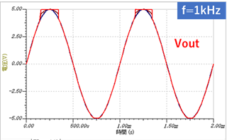
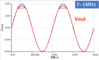
1. Is the NG device output voltage waveform (3ch) shown in the attached document the expected behavior?
2. What is the possible cause of NG device behavior?

<Conditions>

・Voltage Follower Circuit

・Supply Voltage = +-5V

・Input = +-5V, 1kHz

LMH6642MA Waveform.pdf

Best Regards,

Nishie

  • Hi Nishie,

    The NG device output voltage waveform is the expected behavior. The LMH6642 has an input overdrive functionality to avoid output phase reversal. The input overdrive forces the output as close to the supply rail as possible (as dictated by the output voltage limits and the input voltage) when the input Common Mode Voltage Range (CMVR) is exceeded. The CMVR for the LMH6642 is -5.5V to 4.0V. Please refer to section 9.1 and Figure 56 for more details.

    I simulated the circuit in TINA-TI and the results match what you are seeing on the NG circuit. I will attach the simulation for your reference. I will also include an image showing the CMVR and the output waveform. Please let me know if you have any questions.

    LMH6642_Nishie_sim.tdrLMH6642_Nishie.TSC

    Thanks,

    Nick

  • Hi Nick-san,

    Thank you for your support.

    I understood that the operation of the NG device was expected.

    I have another question. Why do OK and NG devices behave differently when operating under the same supply voltage and input conditions? I would like to know what the internal behavior is.

    Best Regards,

    Nishie

  • Hi Nishie-san,

    The CMVR limit for the LMH6642 is 4.0V when running with +/-5V supplies. Since you are driving the input above that limit, the overdrive behavior is seen from some devices like the NG device, but it is possible that some devices are not being overdriven enough to see this behavior like the OK device.

    It is recommended to drive an input that stays within the recommended limits of the device to get stable, consistent results.

    Section 8.2 of the datasheet provides the input equivalent circuit and section 9.1 describes the input overdrive functionality and limitations.

    Thanks,

    Nick

  • Hi Nick-san,

    Thank you for your reply. I understood that both OK and NG device behavior can occur.

    What is the behavior of the input equivalent circuit (section 8.2) when the input overdrive function is worked? I apologize for the lack of study, but I would like to know how the FET and diode of the input equivalent circuit work.

    Best Regards,

    Nishie

  • Hi Nishie-san,

    I believe that you will find section 9.2.1.1 of the datasheet helpful in understanding the behavior of the input equivalent circuit. The input overdrive function occurs when the input voltage range (negative supply - 0.5V to positive supply - 1V) is exceeded by more than a diode drop (or 1Vbe). 

    If there is anything that is still not clear, please let me know.

    Thanks,

    Nick

  • Hi Nick-san,

    I was testing various conditions using the simulation circuit you gave me.

    By increasing the frequency of the input voltage, the operation of the output voltage changed.

    When the input frequency is 1kHz, the output voltage becomes V+. When the input frequency is 1MHz, the output voltage is clamped at about 4V.


    Based on this result, I think there is a difference in the operation of the internal protection circuit depending on the frequency. Could you tell me what part of the internal circuit is affected?

    Best Regards,

    Nishie

  • Hi Nishie-san,

    I am working with the design team to get a better understanding of this behavior. I look to provide you an update no later than early next week. I appreciate your patience.

    Thanks,

    Nick

  • Hi Nick-san,

    I'm looking forward to your reply.

    Best Regards,

    Nishie

  • Hi,

    Thanks for your understanding as I work to get some better answers for you.

    Thanks,

    Nick

  • Hi,

    Sorry for the delay. The LMH6642 is an older design and the design team had to go through a process to get that design. 

    What I can tell you:

    It appears that the difference in behavior vs frequency has to do with how much current is being sourced to the internal protection diodes. If they are not being fully saturated, they may not turn on and drive the output close to the positive supply. The TINA-TI model should be reasonably accurate and should capture the behavior of the LMH6642 pretty well and so I recommend using that to determine what the expected behavior is. 

    With that being said, it is recommended not to drive the input past the CMVR limit. The protection circuit is intended to prevent damage to the device if it is incidentally driven past the voltage range limit and its behavior can not be guaranteed if it is intentionally, continually driven past the voltage range limit.

    Thanks,

    Nick

  • Hi Nick-san,

    Thank you for your support! 

    Best Regards,

    Nishie