This thread has been locked.

If you have a related question, please click the "Ask a related question" button in the top right corner. The newly created question will be automatically linked to this question.

XTR111: Want to confirm the current output range 0-20mA

Part Number: XTR111
Other Parts Discussed in Thread: DAC8551

Hello,

I want to use XTR111 for converting 0V-3V input voltage (Vvin) to 0mA-20mA current output. 

We have below queries:

1. As datasheet mentioned specified output current is 0.1 to 25mA, so can it be possible to use convert this 0mA with 0V input voltage?

2. In our application we are using inbuilt DAC of microcontroller which will give maximum 0.0466V instead of 0V as per its accuracy, which will provide nonzero mA current at output XTR111. Can it be possible to minimize this error? so that we will get 0 mA as starting value.

-- Nikhil 

  • HI Nikhil,

    1.  The XTR111 can produce close to ~0mA output, if 0V input is provided to the device; but there will be a small error due to the offsets of the device.   

    The XTR111 accuracy is specified on the Electrical characteristics table of the datasheet: the internal op-amp of the XTR111 has a  ±1.5mV max input voltage offset error (Vos) , and an offset current (Ios) of 0.02% max at 25mA current span or about ~±5uA offset current). 

    Please keep in mind that the external FET transistor will have some small amount leakage current, and the XTR111 accuracy will be directly dependent on the accuracy/drift and resolution of the signal source input voltage or the accuracy/resolution of the DAC.

    2.  It is possible to obtain about ~0mA output when the DAC can only provide ta minimum voltage of 0.0466V using the level shift/trim circuit shown on the device datasheet on page 17. 

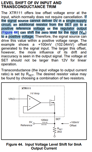
    If the DAC or signal source cannot deliver 0V in a single-supply circuit, an additional resistor from the SET pin to a positive reference voltage or the regulator output (Figure 44) can shift the zero level for the input (VIN) to a positive voltage. This is explained on the section "LEVEL SHIFT OF 0V INPUT AND TRANSCONDUCTANCE TRIM" on page 17 of the datasheet.  The accuracy of this circuit is a function of the tolerance and drift of the resistors and the accuracy of the voltage reference.

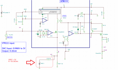
    For example, if you require a 0mA to 20mA  current output, for a DAC input range of +0.0466V to +3V, you could select RSET to 1.5kΩ.

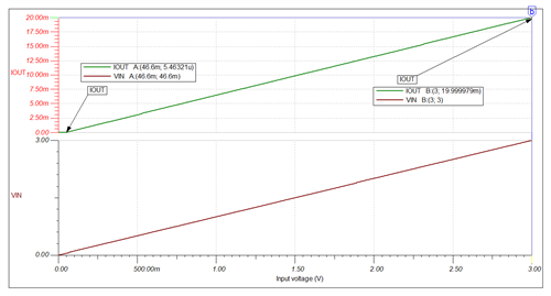
    Since the minimum voltage of the DAC range is 0.0466V, this corresponds to an ISET current of 0.0466V / 1.5kΩ= ~31.6uA. Hence, applying a 3V reference voltage, and 95.3kΩ resistor on RSET as shown below will allow for a 0mA current output for a 0.0466V input, and 20mA current output for a 3V input.  In essence, the 3V reference and 95.3k resistor is injecting a current of ~31uA into the circuit. 

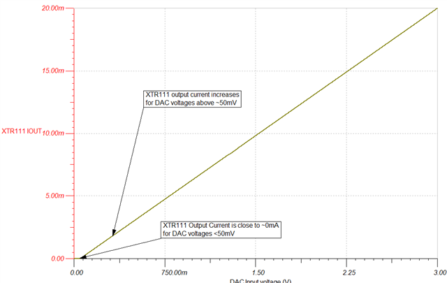
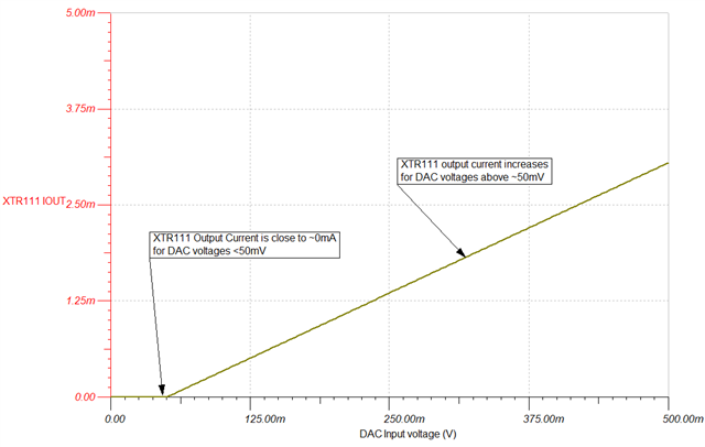
    The below is a quick TINA simulation using a simplified or idealized model to check the circuit transfer function after applying the level shift trim..

    Thank you and Regards,

    Luis

  • Hi Luis,

    For your comment 1: Apart from the above mentioned parameter in accuracy point of view,  RSET resistor value (like resistor tolerance, ppm)  need to be consider for accuracy calculation or not?

    For comment 2: The Vvin voltage is not fixed +0.0466V, it will vary between +0.000713V  to  +0.0466V. In that case how should I get Iout = 0mA at output of XTR111?

    Regards,

    Nikhil

  • HI Nikhil,

    1) Yes, the RSET resistor tolerance accuracy and temperature drift will affect directly the accuracy of the XTR111.  Select a resistor per your accuracy requirements. The transfer function of the XTR111 is IOUT = 10*(VIN / RSET), where the current output is a function of the VIN input voltage accuracy, and the RSET resistor accuracy.

    Review the following XTR111 reference design, it discusses the IOUT accuracy analysis of a XTR111circuit example in great detail accounting for the resistor tolerance, offset, gain error and non-linearity of the XTR111, as well as the errors of the DAC circuit.

    Single-Channel, Isolated, 3-Wire Current Loop Transmitter Reference Design

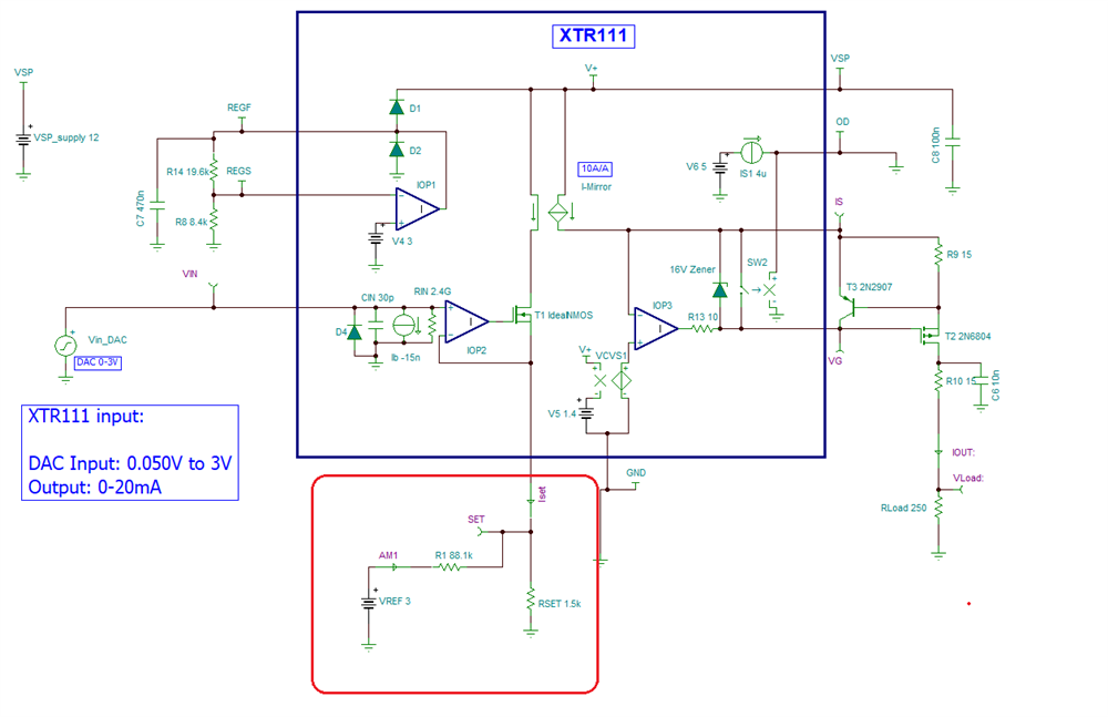
    2) The signal needs to be shifted accounting for the worst case minimum DAC voltage, hence if the minimum DAC voltage may vary the range of +0.000713V  to  +0.0466V; create the offset accounting for the largest minimum DAC voltage in the range. For example, lets assume the largest minimum is ~0.050V for margin, where RSET is 1.5kΩ:  

    - Since the minimum voltage of the DAC range is 0.050V, this corresponds to an ISET current of 0.050V / 1.5kΩ= ~33.3uA. 

    - Applying a precision 3V reference voltage, and using a 88.1kΩ resistor on RSET will injecting a current of 3V/88.1kΩ= ~34uA into the RSET circuit.  The XTR111 will produce close to 0mA for any DAC input voltage smaller than ~50mV.

    Thank you and Regards,

    Luis


  • Hi Luis,

    Thank you for the explanation. We having below query:

    1. As per reference document mentioned by you "">www.ti.com/.../tidub12" for XTR111 accuracy calculations. We have query regarding accuracy calculations of DAC output. Why "VREF initial accuracy" parameter is not considered in equation 3? 

    In our case 1.948 % FSR drift will occur in VREF signal, is this VREF parameter need to consider for accuracy calculations in equation 3 in our case? or it can be removed by calibration?  because DAC Output is depends upon below equation. where VREF = AVCC1.

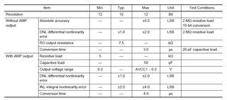
    2. We are using inbuilt MCU (R5F564MFDDFB) DAC which are having below specifications in datasheet

    I am using without AMP DAC output, in that case only Absolute accuracy will came in calculations? 

    Regards,

    Nikhil 

  • HI Nikhil,

    Regarding your question:

    1. As per reference document mentioned by you "">www.ti.com/.../tidub12" for XTR111 accuracy calculations. We have query regarding accuracy calculations of DAC output. Why "VREF initial accuracy" parameter is not considered in equation 3? 

    In our case 1.948 % FSR drift will occur in VREF signal, is this VREF parameter need to consider for accuracy calculations in equation 3 in our case? or it can be removed by calibration?  because DAC Output is depends upon below equation. where VREF = AVCC1

    The reference design document TIDUB12 provides equation (2) for Total Uncalibrated Error, TUE, accounting for the reference initial accuracy:

    Then explains that after applying a two-point best fit calibration to the design to remove the effects of gain an offset errors, and leave only the linearity errors of the DAC8551, as shown on equation (3).

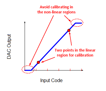
    Essentially, an external high precision meter is used two perform a two point DAC output measurement, one measurement slightly above zero scale and a second point slightly below full-scale, keeping the DAC well inside its linear range.  The offset and gain error of the measured result is compared against the "ideal" result, and in essence the gain error and offset errors of the circuit are measured. In essence, the transfer characteristic is a linear function in the form y=mx +b.  The offset and gain calibration is based on the idea that we can solve the straight line equation for the slope and intercept, where, the slope error is the gain error and the intercept is the offset.

    The reference initial accuracy causes a DAC full-scale error, analogous to gain error or essentially slope in the linear function.  After calibrating, the measured slope and measured offset, called calibration coefficients, are stored in the microcontroller’s memory, and these coefficients are then applied during normal device operation, applying the coefficients to the DAC codes to compensate for the gain and offset error.

    It is important to highlight that the calibration is only effective assuming that the reference, and passive components are very stable over time and have  low drift at the required temperature range, else different calibration coefficients will be required for different temperatures.  It is also very important that the external measurement system (measuring voltage or current during the calibration routine) is considerably more accurate than the targeted accuracy.  If the reference drifts over time or temperature the calibration will be invalid.  

    The TI reference circuit on the application note uses a high precision DAC and a low-drift precision reference that offer low-drift over temperature.

    An excerpt of a presentation is attached discussing the gain and offset calibration for an ADC acquisition system.  The circuit is different than this DAC application, but the same general concepts related to an offset and gain error calibration apply.\

    Calibration_example.pdf

    2) The TI reference design above uses a dedicated/discrete DAC8551 which offers 16-bit precision, and offers a datasheet that specifies much better linearity and lower drift.  In general, the accuracy of the system will be limited by the DAC accuracy/drift; and the voltage reference voltage stability over time and temperature drift.

    As you have mentioned, in your application, the circuit uses a 12-bit DAC peripheral integrated on the  R5F564MFDDFB  microcontroller which will not offer the same level of performance as a discrete, precision16-bit DAC. It may be possible to attempt a level of calibration to reduce gain and offset errors, but keep in mind the calibration is effective to the level of the DAC voltage stability/accuracy/drift over time and temperature, as well as the drift/stability of the DAC reference.  Since this is not a TI device, please consult the microcontroller manufacturer for questions about the DAC performance.

    Thank you and Regards,

    Luis

  • Hi Luis,

    Thank you for explanation.

    Just want to confirm below :

    1. In shared document https://www.ti.com/lit/pdf/tidub12  , in equation-6 considered ITUE_ XTR = 0.036% where as per equation-4 it is 0.034%. Does it Typo mistake or it is addition of equation-4 and equation-5 values?


    2. How the RSET tolerance = 0.03 %FSR is calculated? I have not found it in above mentioned document.

    Regards,

    Nikhil 

  • Hi Nikhil,

    In shared document https://www.ti.com/lit/pdf/tidub12  , in equation-6 considered ITUE_ XTR = 0.036% where as per equation-4 it is 0.034%. Does it Typo mistake or it is addition of equation-4 and equation-5 values?


    The total uncalibrated error of the XTR is ITUE_XTR = 0.034% on this example.  Equation 6 should also use ITUE_XTR = 0.034%.  This is a typo.

    2. How the RSET tolerance = 0.03 %FSR is calculated? I have not found it in above mentioned document.

    This is a direct function of the resistor tolerance spec.

    In this example, the Author is using "Typical" values for error and not worst case "maximum". I believe the Author of the article is using the typical error specific for the resistor manufacturer in use; which is smaller than the ±0.1% min/max tolerance error, and assume the typical (resistor average±1-sigma) is 0.03%.  This approach makes sense if the resistor tolerance offers a Gaussian distribution.

    However, when discussing the resistor tolerance, keep in mind: Resistors provide a percent % max/min tolerance spec for room temperature, and a temperature coefficient in ppm/C. But, resistor datasheets don't always provide a histogram plot of the resistor tolerance nor a typical resistor tolerance spec. The resistor distribution  may vary depending on the specific manufacturer production, testing, and binning processes.  Information about the resistor tolerance distribution may not always be available; and the resistor tolerance may or may not be Gaussian distribution depending on the specific resistor technology or manufacturer production process.  One conservative approach is to assume worst case resistor tolerance. If the resistor manufacturer provides provides a typical tolerance spec, or a histogram with the resistor distribution tolerance is available, then you could estimate the typical resistor tolerance.  You may need to consult with the resistor manufacturer.

    Thank you and Regards,

     Luis