This thread has been locked.

If you have a related question, please click the "Ask a related question" button in the top right corner. The newly created question will be automatically linked to this question.

XTR305: have a pluse when have a input but OD pin is low

Part Number: XTR305
Other Parts Discussed in Thread: XTR300, TIPD155, DAC8563

Hi team,

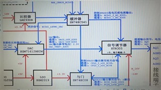
Our customer use XTR305 in such a system, XTR305 input is an DAC signal. When customer OD pin is low,  if DAC has a output, the XTR305 has a small output at the same time .

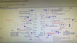
Look the oscillosope waveform, the green is XTR305 output, purple is OD pin.

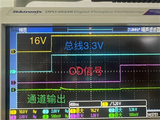
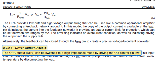
If OD pin is low, XTR305 output shoule be low? Or else?

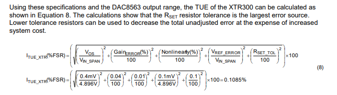
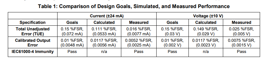
And customer has another question, their DAC precision is 0.1%, but they found XTR305 precision is 0.3%. Is there any methods to make XTR305 output have the same precision like DAC output?

  • HI Minghao,

    1) The XTR305 output is not driven low when the OD is set low. The XTR305 output is set to high-impedance, where the XTR305 output becomes inactive, and the output stage no longer drives or control the output voltage of the device when OD is low. 

    Therefore, any voltage signal, or any glitch seen at the circuit output while OD is set low, is likely caused by external circuitry, or external signals coupling into the XTR305 output through a parasitic paths on the PCB, or through any load or circuitry connected to the XTR305 output; while the XTR305 output stage is high-impedance with the output stage disabled.


    2) Regarding the accuracy of the XTR305, the circuit accuracy is a function of the resistor tolerance and drift, the XTR30x offset voltage, the accuracy of the DAC driving the device, and the VREF reference accuracy error.  The reference design: 'Two-Channel Source/Sink Combined Voltage & Current Output, Isolated, EMC/EMI Tested Reference Design' (TIPD155) documents in good detail the calculation of Total Uncalibrated Error (TUE) for current mode on pages 9-10 for the XTR300. 

    And also provides an example of a Total Uncalibrated Error (TUE) calculation on voltage mode on page 11:

    The reference design shows measured result for unadjusted output current and output voltage, as well as the reduced errors after calibration.

    Note, the reference design discusses the XTR300.  Nevertheless, the XTR300 and XTR305 belong to the same family of devices. The devices are pin-to-pin compatible and offer the same AC frequency response.  The XTR300 device offers slightly better DC precision with a tighter spec for the max gain error, offset error and linearity. The XTR305 is the lower cost version offering more relaxed offset and gain error specifications. Check pages 5,6 on the XTR305 datasheet for the offset, gain error and (non) linearity error specifications, and you can use these parameters on the total error calculations above.

    Please find a link for the TIPD155 reference design below, they discuss the topic in good detail:

    TIPD155 User Guide:

    Two-Channel Source/Sink Combined Voltage & Current Output, Isolated, EMC/EMI Tested Reference Design

    TIPD155 Reference Design web page:
    Two-Channel Source/Sink Combined Voltage & Current Output, Isolated, EMC/EMI Tested Reference Design

    Thank you and Regards,

    Luis

  • Thanks for your answer, but the pluse influence customer system, is there any way to avoid that?

  • HI Yin,

    Yes, as discussed, the XTR305 does not control the output voltage when OD is set low, when the output stage is disabled, and any voltage glitch spike is caused by external circuitry. 

    If the customer needs to drive the output voltage to zero volts while the XTR305 is disabled, then they could consider using an external pull-down resistor to GND, or use an external switch to connect the output of the circuit to GND when the XTR305 is disabled, OR investigate the root cause of the glitch and modify the external circuit that causes the glitch.  The post above does not include a schematic, and has no information about the external circuit that causes the glitch, so it is difficult to comment beyond.

    The XTR305 can only drive the output to zero volts by configuring the XTR device in voltage output mode with OD set high, while driving the XTR305 input with the DAC to produce zero volt output.

    Best Regards,

    Luis

  • Hi Luis, following is customer's schematic diagram.

    And customer found if there is a edge from SET pin, and there will be a pluse in the DRV pin. I and customer both think this is because C50, the capaciance between SET pin and DRV pin.

    And customer's load for XTR305 is that:

    1.for voltage mode their load is a resistance more than 1KΩ with a capaciance 1uF and they hope the rise edge is less than 750us.

    2.for current mode their load is (1).a resistance less than 500Ω with a inductance 1mH and they hope the rise edge is less than 600us. (2).a resistance less than 500Ω with a inductance 10mH and they hope the rise edge is less than 2ms.

    Is there any way can reduce the pluse from customer system?

    I watch the wavefrom the pluse duration is about 100ms. it's a little hard to use a low pass filter to control the pluse.

  • HI Minghao,

    Per your description, you have mention that the pulse is being coupled to the SET pin, and then into DRV through the feedback capacitor.  However, the feedback capacitor C50 is required for XTR compensation so it can not be eliminated.

    One possible suggestion is to increase resistor R41 from 499-Ω to 10-kΩ in an attempt to slow any pulse edge into VIN, in case the pulse is being coupled through a parasitic connections, since the VIN and SET pins are in close proximity.  Another possibility, we could consider adding a small capacitor at the +VIN pin to GND of ~100pF, forming a RC low-pass filter at VIN to slow down any fast pulses into the XTR300 +VIN pin, in an attempt to slow down any fast edges coupling into the SET pin through parasitic paths.

    If the pulse signal is being coupled through a different parasitic path in the PCB board, then we would need to modify the PCB board layout.  If the board layout Gerber files of the DAC - XTR305 section are available, if you wish, we could review the PCB board layout and provide suggestions.

    Thank you and Regards,

    Luis

  • I don't express clearly.

    Customer use an DAC output the reference voltage, so that the DAC output rise edge will influence the DRV pin.

    And I talk with customer about this problem, they want to change the timing, they want give the reference as the same time with XTR305 power on. And it won't influence their system.

    But for precision,is there any way to improve their precision?

  • Minghao,

    Customer use an DAC output the reference voltage, so that the DAC output rise edge will influence the DRV pin.

    - Yes, we suggested using an RC low-pass filter on the VIN path, or in other words, a filter at the output of the DAC, to slow down the rising edge of the DAC output.  This is done in an attempt to reduce the coupling into the RSET signal. However, there may be other paths on the PCB where this signal may be coupled in.  The PCB board layout  and grounding scheme plays a pivotal role in the performance of the circuit 

    And I talk with customer about this problem, they want to change the timing, they want give the reference as the same time with XTR305 power on. And it won't influence their system

    Ok, Thank you.

    But for precision,is there any way to improve their precision?

    - The reference design example includes bench data and detailed analysis and a detailed method to perform a two point calibration. Also includes an optimal board layout example.

    TIPD155 User Guide:

    Two-Channel Source/Sink Combined Voltage & Current Output, Isolated, EMC/EMI Tested Reference Design

    TIPD155 Reference Design web page:
    Two-Channel Source/Sink Combined Voltage & Current Output, Isolated, EMC/EMI Tested Reference Design

    As we discussed, the accuracy of the reference voltage, the DAC voltage accuracy, as well as resistor tolerances and drift influence directly the performance.  The PCB layout plays also a fundamental role in the performance. The XTR300 reference design featured on the app note offers a total uncalibrated error of 0.111% per calculation, and measures 0.025% typical. 

    Note, the TI reference design uses a high precision DAC8563 which offers a high precision output and a high precision reference, It offers a typical DAC error of only 0.0239%.  The voltage reference on the TIPD155 offers a small accuracy error of ±0.1mV typical.  The performance of the DAC and reference are pivotal on the errors above.

    On the partial schematic above, there is no information on the DAC, reference voltage, and there is no information about the conditions nor data in which the accuracy is measured.  Changing the XTR305 to XTR300 will improve the gain error contribution of the XTR form ±0.2% maximum to ±0.12% maximum.  Nevertheless, the overall error will still be a function of the complete circuit including the DAC, reference and all passive components as well as board layout.

    Regards,

    Luis