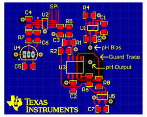
Hi all,
I would like to know the reason that solder mask should not cover the area inside of guard trace.

Is it a noise or leak current measures?
Best Regard,
Ryusuke.
This thread has been locked.
If you have a related question, please click the "Ask a related question" button in the top right corner. The newly created question will be automatically linked to this question.
Hi all,
I would like to know the reason that solder mask should not cover the area inside of guard trace.

Is it a noise or leak current measures?
Best Regard,
Ryusuke.
Hi Ryusuke,
A "Guard" is a driven trace or shield that physically surrounds the input trace and feedback circuitry that is held at a potential equal to the average input signal potential. Since the input circuitry and the guard are kept at the same potential, the leakage current between the two nodes is practically zero. The guard is a low-impedance node, so any external leakages will "leak" into the guard and not into the protected input. This is also the reason why solder mask should not cover the input and the guard area including guard traces on either side of the PCB as the residue left from the solder mask could cause instantaneous current leakage between the guard and the input signal.